
Revolutionizing Antenna Manufacturing: Multi-Material 3D Printing for Next-Gen Wireless Communication (5G, 6G, IoT)
In an era defined by ubiquitous wireless connectivity, the demand for sophisticated and efficient antennas has never been more critical. As our communication methods increasingly rely on wireless technologies, the internet expands its reach into every facet of life, and aerospace applications multiply, the need for lightweight, high-performance antennas has become paramount. The advent of 5G and the impending arrival of 6G have significantly accelerated this requirement, pushing industry players to innovate and find solutions for faster, better, and more cost-effective production. Faced with these challenges, additive manufacturing, particularly multi-material 3D printing, emerges as a transformative technology due to its inherent flexibility and unparalleled ability to create complex geometries. A pioneering team of researchers, led by Xiaoyu (Rayne) Zheng, an Associate Professor in the Department of Materials Science and Engineering at UC Berkeley, has been at the forefront of addressing this urgent need. Their groundbreaking work has culminated in the development of an advanced 3D printing platform designed to facilitate the rapid and precise creation of intricate antenna systems.
The global antenna market underscores the urgency and scale of this innovation. A recent study published by Mordor Intelligence projects that the antenna market is poised to reach an impressive $34.24 billion by 2029, demonstrating a robust annual growth rate of 7.8% over the analysis period spanning 2024 to 2029. This significant growth is a clear indicator of the increasing prevalence and indispensability of antennas across various sectors. Antennas are, without exaggeration, the linchpins of modern communication, serving as essential components in virtually all radio equipment capable of transmitting and receiving energy in the form of electromagnetic waves. This broad category encompasses a vast array of applications, including the rapidly expanding Internet of Things (IoT), cutting-edge 5G and 6G networks, critical satellite communications for global connectivity, and numerous other wireless systems that power our interconnected world. For these diverse applications, the components must adhere to increasingly stringent requirements: they need to be as small and light as possible, yet simultaneously deliver exceptional performance, high efficiency, and rapid data transfer speeds. While traditional manufacturing methods, such as machining, have historically dominated antenna production, 3D printing technologies are rapidly gaining traction. This growing interest is largely attributed to their unique capabilities, particularly the integration of complex lattice structures, which can dramatically reduce the final weight of an antenna without compromising its structural integrity or electrical performance. This opens up new avenues for design freedom and functional integration that were previously unattainable.

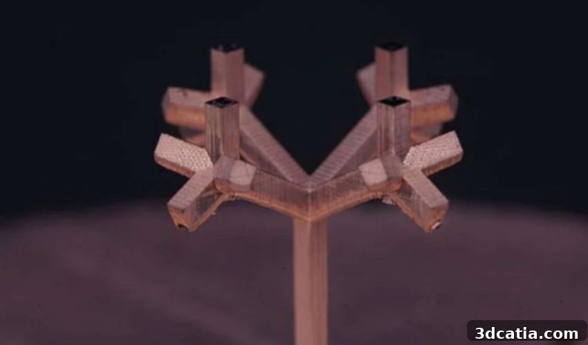
Phase gradient emission grating with three layers of interpenetrating S-rings and dielectric materials (photo credit: X. Zheng)
Overcoming Manufacturing Hurdles: Antennas and the Limits of Current 3D Printing
Despite the immense potential of additive manufacturing for antenna production, the existing technologies on the market have faced significant limitations. One of the primary hurdles lies in the restricted ability to mix diverse materials within a single print process. Typically, manufacturers have been forced to choose between creating an all-dielectric or an all-metal antenna, severely limiting design possibilities and the range of applications that can be realized. Many advanced antenna designs require a precise combination of both conductive metallic elements and insulating dielectric substrates to achieve optimal performance, such as specific impedance matching, beam steering, or frequency tuning. When it has been possible to combine these materials using current 3D printing methods, it often necessitates exceedingly cumbersome and time-consuming post-processing steps. These might include multiple printing stages, complex material preparation, or the use of specialized tooling and substrates that diminish the core advantages of additive manufacturing, such as design freedom and rapid prototyping. In essence, the existing solutions have fallen short of providing a truly integrated, multi-material approach that fully leverages the benefits of 3D printing for high-performance antenna systems. This gap has driven the urgent need for a more comprehensive and versatile manufacturing platform capable of seamlessly integrating different material types.
The Breakthrough: Charge Programmed Multi-Material 3D Printing (CPD)
It was precisely with these critical limitations in mind that Professor Zheng and his dedicated team at UC Berkeley embarked on the development of their revolutionary new 3D printing platform. Named “charge programmed multi-material 3D printing,” or CPD, this innovative system represents a significant leap forward in additive manufacturing. Professor Zheng elaborates on its capabilities, stating, “The new platform—dubbed “charge programmed multi-material 3D printing (CPD)—is a universal system for rapid production of nearly all 3D antenna systems. It can pattern highly conductive metals with a wide range of dielectric materials into a 3D layout.” This statement highlights the core innovation: the ability to intricately combine disparate materials—specifically highly conductive metals and diverse dielectric compounds—within a single, integrated 3D structure. This universality is what distinguishes CPD from previous attempts, promising to unlock unprecedented design flexibility and performance for antenna engineers.
So, what is the underlying mechanism behind this groundbreaking technology? The CPD process ingeniously leverages precise control over charge polarity during multi-material photomonomer printing. The team utilizes an advanced form of stereolithography (SLA), a common 3D printing technique, to strategically deposit various photopolymers in distinct locations within the build volume. Unlike traditional SLA, which typically uses a single photopolymer resin, CPD creates a sophisticated 3D mosaic of different polymer types. These selectively deposited photopolymers are engineered to possess specific charge characteristics. Once the polymer structure is solidified, these charged regions act as highly selective attractors for metal ions. Subsequent metal plating processes then deposit conductive metal onto these charged areas of the 3D polymer structure. This sophisticated interplay between charged polymers and metal ions allows for unprecedented control over the precise design and material distribution of the final antenna. Engineers can now define not only the geometric shape but also the material composition at a micro-scale level, leading to highly optimized and custom-tailored antenna solutions.
The implications of this precise material control are profound. Professor Zheng further emphasizes the versatility of the CPD platform: “It allows essentially any complex 3D structure, including complex lattices, and has demonstrated deposition of copper with near pristine conductivity, as well as magnetic materials, semiconductors, nanomaterials and combinations of these.” This capability addresses several critical aspects of advanced antenna design. The ability to create complex lattice structures is particularly significant, as these lightweight yet robust internal geometries can reduce material usage, minimize overall antenna weight, and even enhance electromagnetic performance by guiding wave propagation. The achievement of “near pristine conductivity” with deposited copper is crucial for minimizing signal loss and maximizing antenna efficiency, which are critical metrics for high-frequency applications like 5G and 6G. Furthermore, the capacity to integrate a broad spectrum of advanced materials—including magnetic materials for tunable antennas, semiconductors for integrated active components, and nanomaterials for novel electromagnetic properties—opens the door to entirely new classes of smart and multifunctional antenna systems. This truly integrated, multi-material approach effectively sidesteps the cumbersome post-processing steps and material limitations that have long plagued additive manufacturing for electronics, pushing the boundaries of what is achievable in antenna design and production.
Future Outlook and Transformative Impact on Wireless Technology
While the team has already made significant strides in the creation of complex antennas, their vision extends even further. Their ongoing research is focused on continually refining the CPD platform with the ultimate aim of making the entire manufacturing process quicker, more efficient, and easier to implement on an industrial scale. This includes optimizing printing speeds, improving material compatibility, and developing more sophisticated software tools for design and simulation. The potential impact of this technology is immense, promising to accelerate the development cycles for new wireless devices and systems across various industries. From enabling smaller, lighter, and more powerful antennas for smartphones and wearables to facilitating the deployment of advanced communication arrays for autonomous vehicles, drones, and satellite constellations, the applications are virtually limitless. The flexibility to rapidly prototype and iterate complex designs will empower engineers to push the boundaries of performance and miniaturization, leading to breakthroughs in fields such as telecommunications, aerospace, defense, and the burgeoning IoT sector. You can find more in-depth information and technical details about this groundbreaking research in the comprehensive study published HERE.
In conclusion, the work by Professor Xiaoyu (Rayne) Zheng and his team at UC Berkeley represents a pivotal moment in the evolution of antenna manufacturing. By overcoming the long-standing challenges of multi-material integration in 3D printing, their Charge Programmed Multi-Material 3D Printing (CPD) platform offers a universal solution for producing high-performance, complex antennas. This innovation is not merely an incremental improvement; it is a fundamental shift that promises to redefine how antennas are designed, prototyped, and manufactured, ultimately paving the way for the next generation of wireless communication technologies that are faster, more reliable, and more deeply integrated into our daily lives. As the world becomes increasingly connected, technologies like CPD will be instrumental in building the invisible infrastructure that powers our digital future, making connectivity seamless and efficient for everyone, everywhere.
What are your thoughts on using advanced multi-material 3D printing to produce high-performance antennas for the future of wireless communication? Let us know in a comment below or connect with us on our LinkedIn, Facebook, and Twitter pages! Don’t forget to sign up for our free weekly Newsletter here to receive the latest 3D printing news straight to your inbox! You can also find all our engaging videos on our YouTube channel.