
DLP 3D Printing Transforms Microfluidic Device Manufacturing for Biomedical Applications
The landscape of medical technology is continually evolving, with breakthroughs in various fields enhancing our ability to diagnose, treat, and understand complex biological processes. Among these advancements, the application of additive manufacturing, particularly in the realm of microfluidics, stands out as a critical area of innovation. Microfluidic devices, often referred to as “labs-on-a-chip,” have gained significant traction over the last three decades due to their ability to manipulate tiny volumes of fluids with unparalleled precision. These compact systems are now indispensable tools in a myriad of biomedical applications, including but not limited to groundbreaking cancer research, efficient drug screening protocols, targeted drug delivery systems, and sophisticated molecular diagnostics. While traditional fabrication methods have long dominated this sector, additive manufacturing technologies are increasingly being leveraged to produce these intricate devices, offering novel advantages in terms of design flexibility, rapid prototyping, and cost-effectiveness. A recent pivotal research paper from the Faculty of Pharmacy at Aristotle University of Thessaloniki, Greece, has notably demonstrated the immense potential of Digital Light Processing (DLP) 3D printing for the precise and efficient fabrication of such vital microfluidic components.
Understanding Microfluidics: A Core Technology in Modern Biomedicine
At its essence, microfluidics is the science and technology of manipulating and controlling fluids at the microscopic scale, typically within channels with dimensions ranging from tens to hundreds of micrometers. This manipulation occurs within specialized devices, primarily known as microfluidic chips, which are essentially a network of minuscule channels etched or molded into a substrate material. The profound appeal of microfluidics stems from several key advantages. Firstly, it enables remarkably fast reaction times due to the short diffusion distances and high surface-area-to-volume ratios inherent in micro-scale environments. Secondly, these systems require minimal sample and reagent consumption, drastically reducing costs and making them ideal for precious or limited biological samples. Finally, microfluidic platforms facilitate high throughput screening and analysis, allowing researchers to conduct numerous experiments simultaneously with greater efficiency. Traditionally, microfluidic devices have been manufactured from materials such as glass, silicon, and polydimethylsiloxane (PDMS). While these materials offer good optical properties and biocompatibility, their fabrication often involves complex, multi-step processes like photolithography and soft lithography, which can be time-consuming, expensive, and require specialized cleanroom facilities. The growing adoption of additive manufacturing, particularly advanced 3D printing techniques, is poised to revolutionize these traditional fabrication paradigms by offering more agile and customizable solutions.
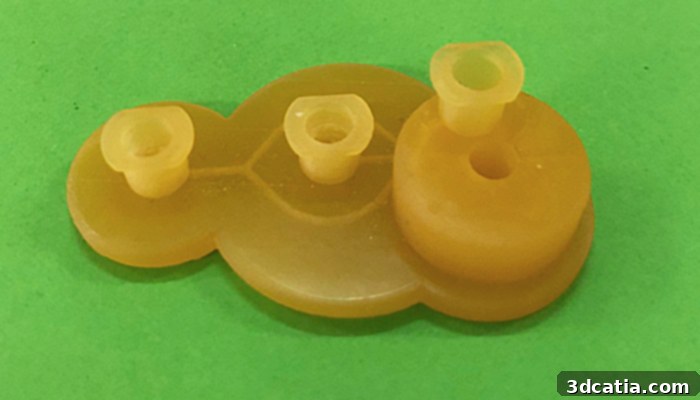
An example of a microfluidic device successfully fabricated by the researchers using DLP 3D printing.
The Evolution of 3D Printing in Microfluidics: From SLA to DLP
For years, the production of microfluidic devices using 3D printing was largely dominated by advanced techniques like Stereolithography (SLA) and Two-Photon Polymerization (2PP). These methods were favored primarily for their exceptional precision and their capability to produce parts with extremely small features and intricate geometries – critical requirements for microfluidic channels. SLA, one of the earliest forms of 3D printing, uses a UV laser to selectively cure layers of photopolymer resin, building up a model point by point. 2PP, an even more precise method, utilizes focused femtosecond lasers to initiate polymerization within the volume of a photosensitive resin, enabling sub-micron resolution. However, these methods often come with trade-offs in terms of speed, material versatility, and equipment cost. The research, titled “Fabrication of a microfluidic device using Digital Light Processing (DLP) 3D printing,” by Eleftherios Andriotis, Paraskevi Kyriaki Monou, and Dimitrios Fatouros, marks a significant milestone by demonstrating that DLP is a powerful and accessible alternative. This pioneering study effectively outlines a methodology for fabricating functional microfluidic devices using DLP technology, a feat accomplished with the invaluable support of Lino3D, a renowned 3D printing laboratory based in Greece, known for its expertise in advancing additive manufacturing education and application.
DLP Technology for Microfluidic Chips: A Detailed Look
For those familiar with the diverse landscape of 3D printing, DLP is recognized as a powerful photopolymerization-based additive manufacturing process. What differentiates DLP from its SLA counterpart lies in its curing mechanism. While SLA employs a focused laser to trace and cure resin point by point, DLP utilizes a digital micromirror device (DMD) – essentially a sophisticated video projector – to project an entire image of each layer simultaneously across the build platform. This fundamental difference allows DLP printers to cure entire layers of photopolymer resin in a single flash, dramatically increasing printing speed compared to laser-based methods, without sacrificing accuracy. EnvisionTEC, now operating as ETEC under Desktop Metal, were the original pioneers and innovators of this technology, developing many of the advancements that define modern DLP printing. It was their expertise and cutting-edge equipment that the researchers from Aristotle University of Thessaloniki turned to for the intricate task of creating their microfluidic devices, leveraging ETEC’s reputation for industrial-grade precision and reliability.
Specifically, the research team opted for the ETEC D4K 3D printer paired with E-RigidForm Amber resin for the fabrication of their microfluidic chips. The choice of E-RigidForm Amber resin was meticulously considered due to its exceptional material properties. This polyurethane-like resin is engineered to produce strong, hard, and stiff end-use parts, making it suitable for functional prototypes and applications requiring robust mechanical integrity. Beyond its strength, the resin exhibits good heat deflection, which is vital for maintaining structural stability under varying operational conditions. Most critically for microfluidic applications, E-RigidForm Amber boasts excellent water resistance. This characteristic is paramount, as microfluidic devices are designed to handle and manipulate aqueous solutions, and any material degradation or permeability by fluids would compromise the device’s functionality and experimental integrity. The D4K printer itself is renowned for its desktop production capabilities, offering extremely high-resolution parts across diverse industries, from intricate jewelry designs to precision dental applications. According to ETEC, the D4K stands out not only for its unparalleled speed among standard DLP printers but also for its ability to deliver remarkably accurate parts with exceptionally fine detail. This attribute proved indispensable for the microfluidic study, given that these devices are constructed on a microscopic scale and involve incredibly intricate channel designs that demand flawless execution for optimal performance.
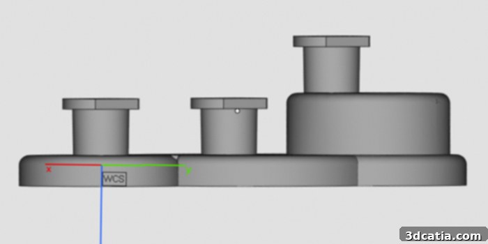
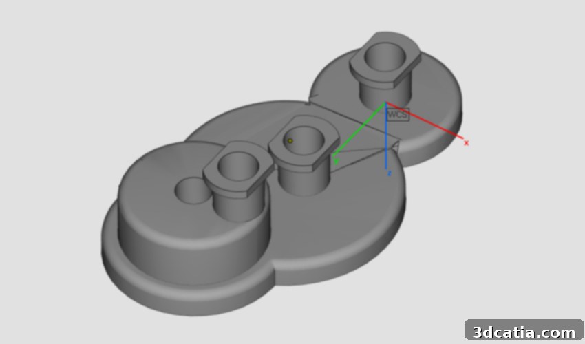
A visual representation of the CAD file, illustrating the complex and precise design of the microfluidic chip.
The Fabrication Process: From Digital Design to Functional Device
The journey from concept to a tangible microfluidic chip involved several critical stages, beginning with meticulous digital design. The researchers initiated the design process using AutoCAD 2019, a powerful CAD software, to create a precise digital model of the microfluidic device. Once the design was finalized, it was exported as an STL (Standard Tessellation Language) file, the ubiquitous format for 3D printing. A crucial aspect of the design involved setting the channel width at a microscopic 700 µm, a dimension that highlights the precision achievable with DLP technology. To ensure practical functionality and seamless integration with external fluidic systems, Luer locks were meticulously incorporated into the inlets and outlets of the design. These standardized connectors are essential for facilitating secure and leak-free tubing connections, enabling researchers to easily introduce and extract fluids from the microfluidic chip. During the printing phase, the ETEC D4K printer was configured with an exceptionally fine layer height of just 1 µm. This ultra-low layer height is paramount for capturing the intricate details of the micro-channels and ensuring the smooth and accurate internal geometries required for effective fluid flow and experimental reliability.
While the printing process itself was a resounding success, demonstrating the DLP printer’s capabilities, a significant post-processing challenge emerged: the removal of residual liquid resin that inevitably blocked the minute inlets and outlets of the newly printed devices. Initial attempts to clean the parts using isopropyl alcohol (99.9%) proved insufficient, as the tiny channels remained obstructed. To overcome this hurdle and ensure the full functionality of the microfluidic chips, the researchers turned to an advanced automated resin removal solution: the DEMI 400 from PostProcess Technologies. This specialized machine employs a combination of proprietary detergents, software-driven agitation, and carefully controlled temperatures to effectively and consistently remove uncured resin from intricate geometries, all while preserving the delicate integrity and fine details of the printed parts. The adoption of the DEMI 400 was a game-changer, allowing the researchers to thoroughly clean the microfluidic chips, clearing all blockages and ensuring the channels were perfectly open and ready for fluid manipulation. The final result was a set of flawlessly fabricated microfluidic devices, a testament to the synergistic power of advanced DLP 3D printing and sophisticated post-processing techniques. This successful demonstration holds immense promise, hopefully paving the way for an even broader adoption of these technologies in fabricating complex devices for a multitude of scientific and medical applications.
Future Implications and the Role of Advanced Additive Manufacturing
The success of this research in utilizing DLP 3D printing for microfluidic device fabrication represents a significant leap forward for biomedical engineering and related scientific disciplines. The ability to rapidly prototype, customize, and produce these intricate chips with high precision and at a potentially lower cost opens up new avenues for accelerating research and development. This methodology can drastically shorten the design-to-experiment cycle, allowing scientists to iterate quickly on new designs and test hypotheses more efficiently. Such advancements are particularly vital in fields like drug discovery, where high-throughput screening on microfluidic platforms can identify potential drug candidates much faster. Similarly, in disease diagnostics, DLP-printed microfluidic devices could enable the development of more sensitive, portable, and cost-effective point-of-care diagnostic tools, bringing advanced medical testing closer to patients. The collaborative spirit between academic institutions like Aristotle University of Thessaloniki and specialized 3D printing labs such as Lino3D (where you can learn more about their instrumental role HERE) exemplifies how interdisciplinary partnerships are driving the future of medical innovation through additive manufacturing. The broader impact of such accessible and precise fabrication techniques on personalized medicine, allowing for patient-specific microfluidic designs, is also immense and points towards a future where medical solutions are increasingly tailored to individual needs.
What are your thoughts on the groundbreaking use of DLP 3D printing for creating highly functional microfluidic chips? We encourage you to share your insights and engage in the conversation by leaving a comment below or connecting with us on our LinkedIn, Facebook, and Twitter pages! Don’t miss out on the latest advancements and news in the 3D printing industry; remember to sign up for our free weekly Newsletter here, delivered straight to your inbox! You can also explore all our informative videos and engaging content on our dedicated YouTube channel.
*All Photo Credits: Lino3D