

Revolutionizing Semiconductor Manufacturing: UT Austin’s 3D Printing Breakthrough
A groundbreaking research team at The University of Texas at Austin has pioneered a novel 3D printing technique poised to reshape the landscape of semiconductor component design and manufacturing. This innovative method, known as Holographic Metasurface Nano-Lithography (HMNL), offers unprecedented speed and complexity in printing chip packages and intricate electronic structures, surpassing the capabilities of traditional manufacturing processes.
Traditional semiconductor fabrication is notoriously slow and costly, involving a protracted sequence of material deposition, masking, etching, and packaging steps. Each stage adds to the overall expense, restricts design flexibility, and generates significant waste. HMNL effectively streamlines this complex workflow by replacing it with a single, efficient 3D printing process capable of patterning advanced electronics in a single pass. This transformative technology enables the fabrication of multi-material, three-dimensional structures that seamlessly integrate metals and high-performance polymers in highly detailed and customized geometries.
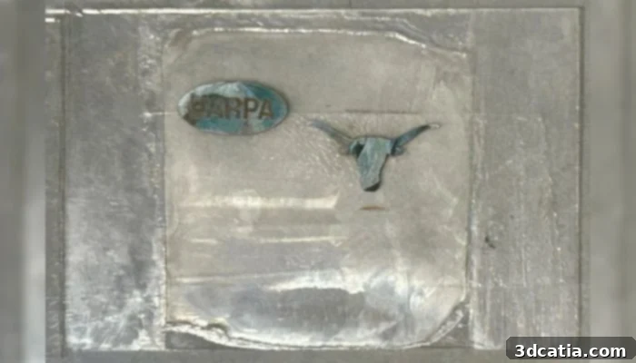
An example of the Holographic Metasurface Nano-Lithography (HMNL) method applied to a semiconductor.
At the heart of the HMNL process lie metasurfaces – ultra-thin optical masks containing densely packed patterns of encoded information. When illuminated, these meticulously designed surfaces project holograms into a specialized hybrid resin. This resin then solidifies, forming precise microstructures with exceptional accuracy. Researchers emphasize that HMNL can achieve feature sizes smaller than a human hair and create intricate forms that are simply unattainable with traditional step-by-step lithography techniques. This opens up exciting possibilities for entirely new component categories, including fully 3D printed capacitors, non-planar chip packages, and electronics custom-shaped to seamlessly integrate into robotics or aerospace systems where space is a critical constraint.
This ambitious project, backed by a substantial $14.5 million grant from DARPA (Defense Advanced Research Projects Agency), benefits from the collaborative expertise of partners spanning both academia and industry. Researchers from esteemed institutions such as the University of Utah, alongside industry leaders like Applied Materials, Electroninks, NXP Semiconductors, Northrop Grumman, Bright Silicon Technologies, and Texas Microsintering, are working cohesively to accelerate the development and rigorous testing of HMNL-based electronics. This collaborative approach ensures a comprehensive and robust path toward commercialization and widespread adoption.

Research and development of HMNL are spearheaded by the Cockrell School of Engineering at the University of Texas at Austin.
Early prototypes have already demonstrated the remarkable versatility of the HMNL technology across a wide spectrum of potential applications. One notable example is a fan-out module specifically designed for consumer electronic devices, showcasing the technology’s ability to create compact and efficient components. Another prototype focuses on high-frequency systems tailored for defense applications, highlighting the potential for creating advanced communication and radar systems. The research team has also successfully printed electronics that conform to curved surfaces and created active packages that seamlessly combine mechanical strength with essential electrical functionality. These innovative designs underscore how 3D printed microscale structures, created with HMNL, can significantly accelerate rapid prototyping cycles, reduce material waste, and streamline complex supply chains, ultimately lowering the environmental impact of electronics manufacturing.
The commercialization pathway for the HMNL technology is being paved by Texas Microsintering Inc., a promising startup founded with the explicit goal of bringing HMNL to the broader market. The company’s strategic plan involves scaling the technique to a point where chip designers can efficiently produce custom electronic packages in a matter of days, a stark contrast to the months typically required using conventional manufacturing methods. This rapid turnaround capability has the potential to revolutionize the design and development process for electronic devices.
In an era where the semiconductor manufacturing industry faces mounting pressure to enhance efficiency while simultaneously supporting increasingly powerful and sophisticated devices, HMNL presents a paradigm shift in how the industry approaches the fundamental building blocks of chipmaking. By seamlessly integrating advanced optics with the precision and flexibility of 3D printing, the research team is firmly positioning additive manufacturing as a viable and compelling tool for the future of electronics production. This innovative approach offers the potential to overcome many of the limitations of traditional manufacturing, paving the way for more efficient, cost-effective, and sustainable electronics manufacturing processes.
The HMNL technique promises numerous benefits, including:
- Faster Prototyping: HMNL significantly reduces the time required to create prototypes, enabling engineers to iterate designs more quickly and efficiently.
- Increased Design Flexibility: The ability to create complex 3D structures opens up new possibilities for electronic device design, allowing for greater customization and optimization.
- Reduced Material Waste: By printing only the necessary material, HMNL minimizes waste compared to traditional subtractive manufacturing methods.
- Lower Manufacturing Costs: The streamlined process and reduced material waste can lead to significant cost savings in electronics manufacturing.
- Improved Performance: The ability to integrate different materials and create optimized geometries can improve the performance of electronic devices.
- Customization: HMNL enables the creation of custom electronic packages tailored to specific applications, providing a competitive advantage.
The potential impact of HMNL on the electronics industry is substantial. It could lead to:
- More powerful and efficient electronic devices: By enabling the creation of more complex and optimized designs, HMNL can contribute to the development of more advanced electronic devices.
- Faster innovation cycles: The rapid prototyping capabilities of HMNL can accelerate the pace of innovation in the electronics industry.
- More sustainable manufacturing practices: The reduced material waste and streamlined processes of HMNL can contribute to more sustainable electronics manufacturing.
- New applications for electronics: The ability to create custom-shaped electronics opens up new possibilities for applications in various fields, including robotics, aerospace, and healthcare.
The University of Texas at Austin’s HMNL technology represents a significant step forward in semiconductor manufacturing. Its potential to revolutionize the industry is undeniable, and its impact is likely to be felt for years to come. As the technology continues to develop and mature, it is poised to play a key role in shaping the future of electronics.
What are your thoughts on UT Austin’s developments? Share your opinions and insights in the comments below. Let’s discuss the potential impact of HMNL on the future of electronics manufacturing.
*All Photo Credits: University of Texas at Austin