
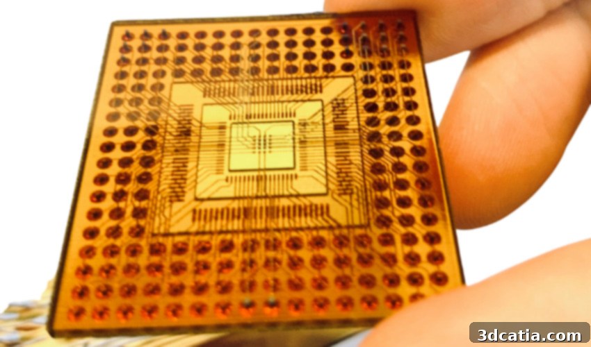
Revolutionizing Electronics: An In-Depth Look at Additive Manufacturing and Nano Dimension’s Vision
Additive manufacturing (AM), commonly known as 3D printing, has emerged as a transformative force across a multitude of industries over the past few years. Its inherent ability to produce highly customizable, topologically optimized, and often more cost-effective components compared to traditional manufacturing methods has cemented AM’s indispensable role in critical sectors such as aerospace, automotive, and medical devices. However, despite its widespread adoption, one industry where AM has historically struggled to gain significant traction is electronics. While the creation of intricate mechanical parts has seen rapid advancements, the complexities of integrating conductive and dielectric materials at a microscale have presented unique challenges for Additive Manufacturing Electronics (AME).
Nevertheless, the landscape is rapidly changing. Recent years have witnessed an exponential growth in microscale additive manufacturing, with dedicated companies tirelessly working to push the boundaries of AME technology. At the forefront of this pioneering movement is Nano Dimension. This innovative manufacturer specializes in advanced 3D printed electronics systems, utilizing their proprietary inkjet printing technology and specialized nano-inks to craft ultra-precise electronic parts. These cutting-edge components serve a diverse range of high-demand industries, including medical, automotive, and aerospace, demonstrating the vast potential of their solutions.
Beyond their revolutionary technology, Nano Dimension is also widely recognized for its substantial contributions to fostering research and collaborating extensively with academia. Their efforts are pivotal in redefining our understanding of AME technologies and expanding the realm of what is possible to create. To gain deeper insights into their groundbreaking technology, the diverse applications of 3D printed electronics, and their strategic engagement with academic institutions to advance existing boundaries and nurture the next generation of engineering talent, we had the privilege of speaking with Valentin Storz, the General Manager of EMEA at Nano Dimension.
3DN: Can you introduce yourself and elaborate on your connection to additive manufacturing?
 My name is Valentin Storz, and I am based in Germany. For the past two and a half years, I have proudly served with Nano Dimension, contributing to our mission of electrifying additive manufacturing. Prior to joining Nano Dimension, I dedicated six transformative years to overseeing European operations for Makerbot and Stratasys. This period was particularly dynamic, highlighted by Stratasys’ acquisition of Makerbot in 2014. That was a truly pivotal moment, as the entire landscape of 3D printing, from its technological capabilities to its market perception and industrial applications, looked significantly different than it does today. My journey in additive manufacturing has provided me with a unique perspective on its evolution, from its early stages in rapid prototyping to its current trajectory towards industrial production and, now, its profound impact on electronics.
3DN: What can you tell us about Nano Dimension? How did it begin, and what drives its core mission?
Nano Dimension stands as the pioneering company dedicated to electrifying additive manufacturing, fundamentally transforming how we conceive and produce electronic devices. Our core innovation lies in a sophisticated system, aptly named DragonFly LDM®, which is roughly the size of two refrigerators. This powerful system possesses the unique capability to simultaneously jet both dielectric and conductive nano-inks, enabling the precise 3D printing of complex, free-form electronic parts. Essentially, we are bridging a critical technological gap that traditionally exists between the rigid limitations of the Printed Circuit Board (PCB) industry and the intricate demands of the Semiconductor Industry. We achieve this through the development of what we call Hi-PEDs™ (High-Performance Electronic Devices).
These Hi-PEDs™ are far more than just conventional circuit boards with printed components. They represent a paradigm shift, allowing for the direct additive manufacturing of highly integrated functional electronic devices. This includes embedding passive and active components such as coils, capacitors, transformers, and incredibly complex multi-layered circuitry directly within a single, integrated structure. Our technology unlocks unprecedented design freedom, enabling engineers to create electronic devices that are smaller, lighter, and more efficient than previously possible with traditional methods. Our involvement spans numerous critical projects and high-stakes industries. A notable example of our capabilities is the 3D printed Radio Frequency (RF) Amplifier we produced, which successfully journeyed to the International Space Station – a testament to the reliability and performance of our additive manufacturing electronics in extreme environments. The overarching mission of Nano Dimension is clear and ambitious: to revolutionize electronics additive manufacturing, making advanced electronic devices accessible, customizable, and more powerful than ever before.
3DN: Could you elaborate further on your Lights-Out Digital Manufacturing (LDM) technology and specifically on the DragonFly LDM Manufacturing System?
The DragonFly LDM® system is at the core of our innovation, equipped with our state-of-the-art, proprietary Lights-Out Digital Manufacturing (LDM) technology. This technology is a game-changer for the production of Additive Manufacturing Electronics. LDM enables truly unattended operation, fundamentally transforming the traditional manufacturing workflow. Unlike many conventional systems that require frequent manual intervention, the DragonFly LDM® system is designed to maintain itself, typically requiring only one weekly maintenance operation. This drastically reduces labor costs, increases operational efficiency, and allows for much higher production throughput.
Currently, the DragonFly LDM® stands as the industry’s only comprehensive additive manufacturing solution specifically engineered for the around-the-clock 3D printing of electronic circuitry. This unparalleled capability is the result of significant technological advancements and iterative improvements integrated into the system. Key innovations include a new, highly advanced printer head that ensures consistent, precise material deposition; sophisticated software management algorithms that optimize printing parameters and monitor system performance in real-time; and an automatic self-cleaning mechanism for the print heads, which activates every few hours to prevent clogging and ensure uninterrupted operation. This robust combination of features allows the DragonFly LDM® to operate with minimal human oversight, maximizing uptime and productivity.
At its heart, the DragonFly LDM® is a highly precise inkjet deposition printer. It utilizes dedicated nano-inks, meticulously formulated for their dielectric and conductive properties, in conjunction with optimized 3D software specifically developed for printing complex electronic circuits. This synergy between hardware, materials, and software sets new precision standards for 3D printed electronics, allowing for incredibly fine features and intricate multi-layered designs that were previously unattainable. The LDM technology not only ensures superior quality and repeatability but also ushers in a new era of agile manufacturing for electronic devices, where designers can rapidly iterate and produce functional prototypes and end-use components with unprecedented speed and efficiency.
3DN: What are the primary applications of this revolutionary technology in the field of Additive Manufacturing Electronics?
The applications for Additive Manufacturing Electronics (AME) are incredibly diverse and continue to expand as the technology matures. While the production of Printed Circuit Boards (PCBs) is an obvious and significant application, our technology truly excels in the realm of advanced Radio Frequency (RF) solutions. This includes the rapid prototyping and production of highly specialized components like Omni Antennas, which can be custom-designed for specific directional properties and integrated directly into devices, enhancing performance and reducing form factor. We’re also seeing significant potential in the development of cutting-edge 5G components, Micro-Electro-Mechanical Systems (MEMS), and highly sophisticated Advanced Sensors. The ability to create Non-Planar Multi-Layer Electronics and High-Density Interconnect (HDI) structures with ease offers unparalleled design freedom, allowing for complex geometries and improved signal integrity that are challenging or impossible with traditional planar manufacturing techniques.
The beauty of our system lies in its simplicity and flexibility: users can simply input their desired specifications, define the intricate shape and functionality, and the system is ready to print with minimal setup. This agility offers immense advantages for RF technology development, where rapid iteration and customization are paramount. Beyond RF, our technology is also highly valuable for innovative packaging solutions, enhancing the protective and functional aspects of electronic enclosures. It’s also being utilized for IC shielding, providing integrated electromagnetic interference (EMI) protection directly during the printing process, and for creating integrated sensors. Touch sensors, for instance, are an increasingly important application, offering seamless integration into a wide array of devices across the medical, industrial, and automotive fields, enabling new levels of human-machine interaction and data collection.
It’s important to acknowledge that AME is still a relatively young technology within the broader additive manufacturing landscape. Consequently, a significant portion of its current adoption is focused on research and development purposes. Because of this, Nano Dimension is actively prioritizing the empowerment of researchers and academics. We are observing a rapid proliferation of publications and studies in the field, indicating a strong and growing interest from these sectors. By enabling cutting-edge research, we are not only proving the capabilities of our technology but also helping to uncover new, unforeseen applications and push the boundaries of what 3D printed electronics can achieve. This collaborative approach with the academic community is essential for accelerating the maturity and broader industrial adoption of AME.
3DN: What do you foresee as the next significant steps in 3D printing technology, particularly concerning the evolution of the AM electronics market over the coming years?
Looking ahead to the next few years, I anticipate a profound and growing influence from several key sectors on the evolution of 3D printing technology, especially within the AM electronics market. We will undoubtedly see increased adoption and innovation stemming from research academia, pushing the theoretical and practical limits of what’s possible. The defense sector will continue to be a significant driver, requiring highly specialized, durable, and customized electronic components for advanced military applications. Similarly, the medical field will leverage AME for bespoke implants, wearable sensors, and complex diagnostic devices that demand extreme precision and biocompatibility. Beyond these, other highly specialized solutions across various industries will increasingly turn to AME for tailored electronic parts that traditional manufacturing cannot provide.
When we consider the market for Printed Circuit Boards (PCBs), it currently stands as a massive $7-billion-dollar industry. However, this figure merely represents the apex of the broader electronics industry pyramid. There’s an even more specialized, high-value segment of the industry that AME is perfectly positioned to address. This segment demands innovation in areas such as new form factors – moving beyond flat, rigid boards to create electronics that conform to complex, three-dimensional designs. Miniaturization will continue to be a critical trend, driving the need for smaller, more compact, and higher-performance devices. Furthermore, we will witness a greater integration of assembly steps and components directly into the 3D printing process, significantly streamlining manufacturing and reducing reliance on manual assembly.
Ultimately, the widespread adoption of digital inventory will revolutionize supply chains. Instead of warehousing physical components, companies will store digital designs, printing parts on demand as needed. This not only reduces waste and inventory costs but also enables unparalleled agility and customization. These advancements—new form factors, miniaturization, integrated assembly, and digital inventory—will collectively pave the way for a deeper and more pervasive development of electronics within the additive manufacturing paradigm. The ability to innovate at every layer, from materials to design and functionality, means that the AM electronics market is poised for explosive growth and will redefine the capabilities of future electronic devices.

Nano Dimension also has a 3D printing service, NaNoS℠ (photo credits: Nano Dimension)
3DN: What is the crucial importance of academia’s role, especially when it comes to electronics design and educating the next generation of engineers in AME?
Education is not just important; it is absolutely crucial in the additive manufacturing field, and this sentiment is amplified exponentially when we delve into Additive Manufacturing Electronics (AME). The stark reality today is that very few engineers are formally trained in designing for AME technology. As a direct consequence of this educational gap, many professionals and aspiring engineers instinctively approach design problems through the lens of traditional manufacturing methods, which inherently limits their creativity and restricts innovation to established boundaries. With AME, however, the industry is dealing with entirely new machines and processes that demand a fundamentally different approach to design development, a deep understanding of novel materials, and an appreciation for integrated systems. Traditional methods are inherently limiting because they are largely planar, making true three-dimensional electronic structures difficult or impossible to achieve.
Encouragingly, a new generation of engineers is emerging, and they are actively pushing the boundaries, championing the adoption of 3D electronics. They are keenly exploring the unprecedented opportunities that AME offers and are consistently generating groundbreaking new ideas. Recognizing this imperative, Nano Dimension has made it a core mission to actively collaborate with universities and the broader industry. We are deeply involved in developing and supporting programs designed to advance these essential educational initiatives. Frankly, we all, as an industry, need to do considerably more to foster this growth.
To facilitate this educational and research advancement, we offer more than just our cutting-edge DragonFly LDM® machine, which represents a significant investment at approximately $500,000. We also provide a vital service called NaNoS℠ (Nano Dimension On-Demand Service). Through NaNoS℠, students and professors gain invaluable access to our advanced technology, allowing them to test concepts and validate whether their innovative ideas can be successfully realized using 3D printing technology for electronics. NaNoS℠ functions as a cooperative design and fabrication service, specifically tailored for anyone eager to explore the future of AME fabrication. It empowers professionals, researchers, and students to experiment freely by designing and creating their own Hi-PEDs™ (High-Performance Electronic Devices) and then test-printing them on a diverse range of substrates, including traditional FR4, Silicon, Copper foil, and other novel materials. Our philosophy is one of open innovation: we don’t always know precisely which research paths will yield the most successful outcomes, but we are absolutely committed to providing the tools and support necessary to help advance the field wherever and whenever we can. This collaboration is key to unlocking the full potential of 3D printed electronics and shaping its future.
3DN: Do you have any final thoughts or words of advice for our readers regarding the future of Additive Manufacturing Electronics?
I firmly believe that the transformative impact of additive manufacturing will ultimately be far greater and more profound on the electronics world than even on the mechanical world. While mechanical additive manufacturing has revolutionized prototyping and specialized component production, the ability to fundamentally redesign, miniaturize, and integrate complex electronic functions into entirely new form factors offers a level of innovation that touches every aspect of modern technology. The convergence of hardware and software, enabled by AME, will lead to devices that are smarter, more efficient, and more seamlessly integrated into our lives. I encourage everyone to explore this exciting field. You can find more comprehensive information about Nano Dimension and our groundbreaking technologies on our official website, or by watching the insightful video provided below.
What are your thoughts on Nano Dimension’s pioneering work and the future of Additive Manufacturing Electronics (AME)? We invite you to share your insights and comments below, or engage with us on our Linkedin, Facebook, and Twitter pages! Don’t miss out on the latest advancements and news in 3D printing – sign up for our free weekly Newsletter here, delivered directly to your inbox. You can also explore all our informative videos on our dedicated YouTube channel for more in-depth content.
Thumbnail Photo Credits: Nano Dimension