
Unlocking Peak Performance: How Stabilizer Residues Impact Conductivity in 3D Printed Electronics
The groundbreaking field of additive manufacturing, particularly in the realm of electronics, promises unprecedented innovation and design freedom. However, a significant hurdle has long plagued the development of high-performance 3D printed electronic devices: suboptimal electrical conductivity, especially in the vertical direction. For years, the prevailing belief attributed this challenge to issues concerning the shape and physical continuity at the interfaces of the constituent nanoparticles, particularly at the intricate micro and nanoscale levels. This assumption suggested that the structural integrity and arrangement of these tiny particles were the primary culprits behind reduced conductivity.
Yet, recent research from the esteemed University of Nottingham has unveiled a paradigm-shifting discovery, challenging this long-held notion. Their comprehensive study, meticulously conducted using silver nanoparticles, definitively demonstrates that the principal cause of diminished vertical conductivity in 3D printed electronics is, in fact, the presence of organic chemical residues found within the manufacturing inks. This revelation redirects the focus from purely physical and structural issues to the subtle yet critical chemical composition of the materials used, opening new avenues for optimizing the performance of these advanced devices.
Metal nanoparticle inks stand as one of the most widely adopted conductive materials for fabricating printed electronics, offering a versatile foundation for a myriad of applications. The process typically involves inkjetting successive layers of these metallic nanoparticle materials. This advanced technique allows developers to achieve remarkable design flexibility, significantly accelerated processing times, and the capability to directly 3D print fully functional electronic components. These components span a vast array of critical applications, including sophisticated sensors for various industries, efficient solar panels for sustainable energy, vibrant LED displays, high-speed transistors, and even cutting-edge smart textiles that integrate electronics seamlessly into everyday wear.
The fundamental mechanism behind the formation of solid printed objects through inkjet 3D printing of metals involves a two-stage process. Firstly, upon printing, the solvent within the ink rapidly evaporates, a crucial step often referred to as “pinning.” This initial evaporation stabilizes the deposited material and prepares it for the subsequent consolidation phase. The second stage, known as sintering, involves the low-temperature consolidation of the nanoparticles. This low-temperature requirement is of paramount importance in numerous applications, particularly where nanoparticles are co-printed alongside other functional or structural organic materials that are inherently sensitive to elevated temperatures. Ensuring low-temperature processing is thus cardinal for preserving the integrity and functionality of these heat-sensitive components, making the optimization of this sintering process a key area of research and development.
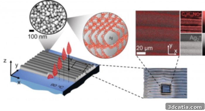
(left) Digital inkjet printing of inks containing metal nanoparticles with in-situ solvent evaporation (pinning). (right) Optical and chemical images of a printed layer of silver nanoparticles showing organic residues at the surface. (Photo Credit: Gustavo Trindade)
Despite the numerous advantages, inkjet printing of metal nanoparticles has historically encountered a persistent challenge known as functional anisotropy. This phenomenon manifests as a significant disparity in electrical conductivity between the horizontal and vertical directions within the printed layers. Essentially, electrons find it much harder to travel from one layer to the next (vertically) than to move within a single layer (horizontally). This longstanding issue has severely hindered the widespread adoption of 3D printing technology for advanced electronic applications, limiting the complexity and efficiency of the devices that can be produced. It has been a bottleneck preventing 3D printed electronics from achieving the performance benchmarks required for competitive integration into modern high-tech systems.
As Dr. Gustavo Trindade, a CfAM Research Fellow and the study’s lead author, elucidates, “The conductivity of inkjet-printed metal nanoparticles is known to be dependent on processing temperature and have been previously attributed to changes in the shape and porosity of clustered nanoparticles, with the role of organic residues being only speculated.” This quote underscores the prior focus on physical morphology and the speculative nature of the role of organic chemicals. The Nottingham study transforms this speculation into concrete evidence. These organic residues, though intentionally incorporated into the inks for the crucial purpose of stabilizing the nanomaterials and preventing their aggregation during storage and printing, unfortunately, have a detrimental side effect. They form ultra-thin, low-conducting nanoscale layers that act as insulating barriers. These nanoscale interferences significantly impede the vertical flow of electrical current through the printed sample, directly contributing to the observed functional anisotropy and limiting the overall performance of the 3D printed electronic device.
With this newfound and clearer understanding of how these residual organic additives are distributed and behave within the printed layers, the research team is now poised to forge ahead. They believe this insight is the key to defining novel techniques and developing revolutionary new ink formulations specifically engineered to overcome the persistent challenge of functional anisotropy in inkjet-based 3D printed electronics. This involves a multi-faceted approach, potentially exploring alternative stabilizing agents, optimizing ink purification methods, or developing post-printing treatments that can effectively remove or neutralize these insulating organic layers without compromising the structural integrity of the printed device.
Dr. Trindade enthusiastically concludes, “This new insight enables the development of routes to overcome functional anisotropy in inkjet-based nanoparticles, and will therefore improve uptake of this potentially transformational technology, making it competitive with conventional manufacturing. Our approach is transferable to other nanomaterial-based inks including those containing graphene and functionalized nanocrystals, and will enable the development and exploitation of both 2D and 3D printed electronics like flexible and wearable sensors, solar panels, LED displays, transistors and smart textiles.” This statement highlights the profound implications of their work. By making 3D printed electronics truly competitive with traditional manufacturing methods in terms of performance and reliability, this research promises to accelerate the adoption of additive manufacturing across various high-tech sectors. The ability to produce electronics with uniform and high conductivity will unlock a wealth of applications that were previously impractical or impossible.
The versatility of this discovery extends far beyond silver nanoparticles. The team anticipates that their approach is readily transferable to a broad spectrum of other nanomaterial-based inks. This includes cutting-edge materials like graphene, known for its exceptional electrical properties, and various functionalized nanocrystals, which possess unique optical and electronic characteristics. This broad applicability signifies a universal solution to a widespread problem in nanomaterial printing. Consequently, this research is set to catalyze the development and widespread exploitation of an exciting array of both 2D and 3D printed electronic devices.
Imagine the possibilities: next-generation flexible and wearable sensors that seamlessly integrate with our bodies or environments, providing real-time data for health monitoring, athletic performance, or structural integrity. Envision highly efficient, conformable solar panels that can be integrated into curved surfaces or lightweight structures, revolutionizing energy harvesting. Picture advanced LED displays that are thinner, more flexible, and consume less power, opening doors for innovative consumer electronics and architectural lighting. Consider breakthroughs in transistors, leading to smaller, faster, and more powerful microprocessors. And finally, the realization of truly smart textiles that can sense, communicate, and adapt, transforming industries from fashion to defense with integrated electronic functionalities. This research paves the way for a future where electronic functionality is not constrained by rigid, planar designs but can be custom-printed into virtually any shape or form, revolutionizing countless industries and enhancing our daily lives.
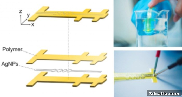
A multi-material inkjet 3D printed prototype of an encapsulated strain sensor used in the study. (Photo Credit: Gustavo Trindade)
This pivotal research by the University of Nottingham marks a critical juncture in the evolution of 3D printed electronics. By accurately identifying the root cause of functional anisotropy, the team has provided a clear roadmap for developing solutions that will unlock the full potential of this transformative technology. Their work promises to usher in an era where high-performance, complex electronic devices can be produced with unprecedented flexibility and efficiency, challenging conventional manufacturing norms and driving innovation across a multitude of sectors. The journey towards truly integrated and highly conductive 3D printed electronics has just received a significant boost, bringing the future of smart, customizable devices much closer to reality.
If you want to find out more information about this groundbreaking study, you can read the full press release HERE. What are your thoughts on this exciting new research from the University of Nottingham? We’d love to hear your perspective! Let us know in a comment below or join the conversation on our Facebook,Twitter andLinkedIn pages! Don’t miss out on the latest advancements in additive manufacturing – sign up for our free weekly Newsletter here, delivering the most up-to-date 3D printing news straight to your inbox!
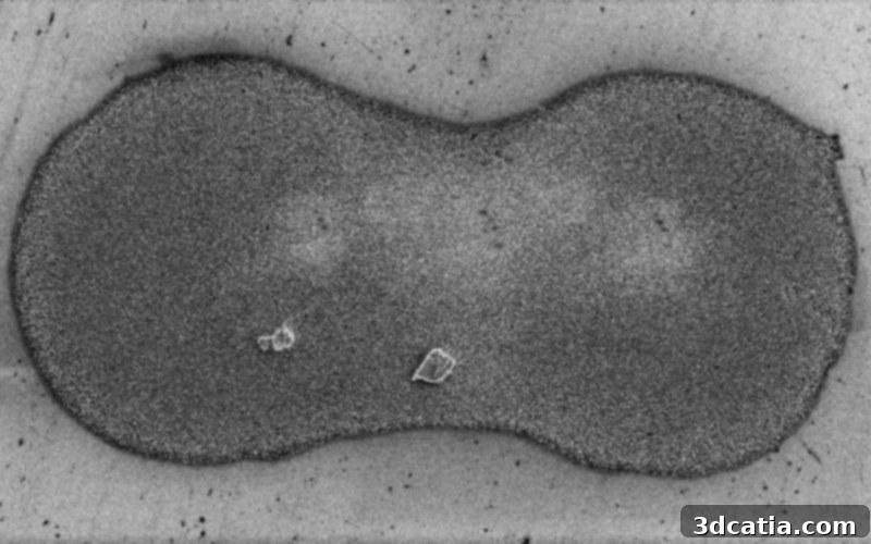
*Cover photo shows a pair of inkjet printed droplets with silver nanoparticles, courtesy of Gustavo Trindade.