

The Power of Precision: Unlocking Miniaturization with Microscale 3D Printing and Nanofabrication
Microfabrication, the art and science of creating minuscule structures at micrometer scales and beyond, has been a driving force behind technological advancement for decades. Its origins are deeply rooted in the electronics industry, where the relentless pursuit of smaller, more powerful devices transformed the landscape of modern technology. Over the years, we’ve witnessed electronic gadgets shrink from bulky devices to sleek, pocket-sized marvels. This miniaturization journey saw component sizes decrease from tens of micrometers to single-digit micrometers, then hundreds of nanometers, and now down to just a few tens of nanometers. This incredible progression has led to the rebranding of traditional microfabrication as nanofabrication, even though the fundamental principles governing these processes largely remain consistent. To continuously meet the demanding challenge of shrinking component sizes, especially in microelectronics, researchers and engineers are constantly developing innovative tools and techniques. Among these groundbreaking approaches, microscale 3D printing stands out as a particularly transformative technology. But what exactly are the applications enabled by microscale additive manufacturing, and what significant benefits does this cutting-edge micro 3D printing technology offer across various sectors?
Interestingly, within the vast landscape of additive manufacturing, the electronics industry has historically been one of the slower sectors to fully embrace and integrate 3D printing technology. While industries like aerospace pioneered the adoption and development of 3D printing for complex parts and rapid prototyping, electronics initially lagged behind. However, this trend is rapidly shifting as additive manufacturing demonstrates its immense potential to introduce unprecedented benefits and capabilities to the electronics sector. By enabling a new level of customization and complexity for micro and nanoscale components, 3D printing is poised to revolutionize the design and production of electronic devices. It offers the flexibility to create intricate geometries and integrated functionalities that were previously impossible or prohibitively expensive with traditional manufacturing methods.

To meet the continuing challenge of shrinking component size in microelectronics, new tools and techniques are continuously being developed. The main driver of this technology being integrated circuits, such as the one above.
While microscale additive manufacturing was initially conceived and developed with a primary focus on benefiting the electronics industry, the capabilities of this technology are now extending far beyond this initial scope. Today, its potential applications are expanding into diverse fields such, as healthcare and specialized optics. For instance, in the medical sector, nano-sized components fabricated using micro 3D printing could be designed to operate within the human body for targeted drug delivery, advanced diagnostics, or even to cure diseases at a cellular level. Similarly, the creation of highly precise micro-optical elements for various imaging and sensing applications is another promising area. In the following sections, we will delve deeper into the multifaceted relationship between advanced additive manufacturing techniques and micro/nanofabrication. Our goal is to provide a comprehensive overview of the current state of this remarkable technology, exploring its core principles, the innovative tools driving its progress, and its ever-growing range of applications both within and beyond the critical electronics sector.
The Innovative Technologies Behind Microscale 3D Printing
To truly appreciate the transformative potential of microscale 3D printing, it’s essential to understand the underlying technologies that make it possible. One of the primary techniques is known as microstereolithography (micro-SLA), a sophisticated advancement rooted in the principles of conventional stereolithography (SLA). SLA holds historical significance as the very first 3D printing technology to be patented. Microstereolithography operates on a similar manufacturing principle: the selective polymerization of a photosensitive liquid resin by ultraviolet (UV) light. However, it incorporates significant process improvements and specialized optical systems that yield dramatically superior resolution, often achieving feature sizes down to a mere couple of micrometers. This enhanced precision is crucial for fabricating the intricate, miniature structures required for micro and nanoscale applications.
Within the demanding electronics segment, the fabrication process faces a unique challenge: the need to create structures that exhibit both conductive and insulating properties simultaneously. This duality is a complex engineering hurdle. Leading innovators like Nano Dimension, a prominent manufacturer of 3D printed electronic components, have risen to this challenge with their proprietary inkjet 3D printing technology. This system utilizes specialized nano-inks. Building on the principle of photopolymerization, a precision printhead strategically deposits dielectric nanoparticles, conductive nanoparticles, and polymer materials onto a build plate. These layers are then meticulously cured by UV light in between successive depositions, allowing for the precise layering of different materials with distinct electrical properties. Another pioneering company in 3D printed electronics, Optomec, has developed the Aerosol Jet 3D printing technology. This method works by depositing an extremely tight, highly focused stream of electronic inks, capable of creating conductive traces and features as fine as 10 micrometers (µm). Both approaches offer unparalleled control over material placement, enabling the fabrication of advanced electronic circuits and components with integrated functionalities.
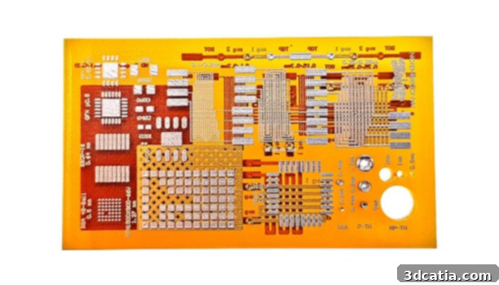
There is a great demand for printed circuit boards (PCBs) to become denser and more complex. The following PCB is multi-layer which means it contains multiple layers of conductive traces instead of containing only 1 | Credits: Nano Dimension
When the application calls for fabricating microstructures from metals, microstereolithography is generally not the most suitable option due to material limitations. For metallic micro-components, specialized additive manufacturing techniques have emerged. Micro laser sintering, for example, is a technology analogous to Selective Laser Sintering (SLS) but optimized for creating remarkably small, intricate metal 3D printed structures. This process is employed by innovative companies such as 3D MicroPrint, based in Germany, which focuses on producing high-precision metallic micro-parts for various industries. On the other hand, Exaddon utilizes a unique process that can be likened to Directed Energy Deposition (DED), which they have named electrochemical deposition. This highly precise method involves a micro-sized nozzle depositing a liquid solution containing metal ions. Through an electrolytic process, triggered by an electric charge, these metal ions are transformed into solid atoms, meticulously building up complex metallic structures with extreme accuracy. These varied approaches highlight the engineering ingenuity required to print with different materials at such minute scales.
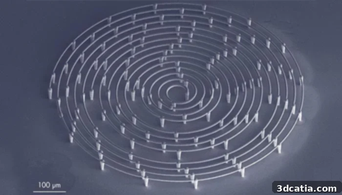
Manufacturing coils with a diameter less than 300 micrometers is a complex challenge which is hardly addressed by conventional methods. The following copper coils have been 3D printed by Exaddon in collaboration with Harvard Medical School | Credits: Exaddon
Delving even further into the realm of the miniscule, nanoscale 3D printing is predominantly achieved through a sophisticated technique known as multiphoton lithography (MPL), most commonly referred to as two-photon polymerization (2PP). As its name implies, 2PP leverages the two-photon absorption phenomenon using high-intensity lasers, typically in the near-infrared (NIR) spectrum. These powerful, focused lasers enable the creation of features with resolutions as fine as an astounding 50 nanometers (0.05 µm). While these parts are incredibly tiny and detailed, their fabrication often takes more time than one might initially anticipate. The process is inherently lengthy because it polymerizes exceptionally small volumes at a time, making it challenging to scale up for larger-volume production. To provide some context, the average human eye can discern objects as small as approximately 0.1 millimeters, which is roughly 100 micrometers (µm). This means that many of the astonishing structures fabricated by two-photon polymerization (2PP) are far too small to be visible without the aid of specialized microscopy.
The pursuit of advancing 2PP technology is a vibrant area of research in numerous universities worldwide. Recently, a significant breakthrough was achieved at the Chinese University of Hong Kong (CUHK), in collaboration with Lawrence Livermore National Laboratory. Researchers there have been dedicated to enhancing the speed and efficiency of 2PP. Dr. Sourabh Saha, who leads this innovative research project, elucidated their achievement: “Traditionally, there are inherent tradeoffs between speed and resolution in 3D printing. If you prioritize a faster process, you often sacrifice resolution. We have successfully broken this engineering tradeoff, enabling us to print structures a thousand times faster while maintaining the smallest possible features.” This remarkable improvement was achieved by replacing the conventional singular high-intensity laser with a field of light, dramatically accelerating the polymerization process without compromising the unparalleled precision that 2PP offers. This advancement is critical for making nanoscale 3D printing more viable for broader applications and potential industrial scale-up.
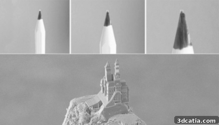
This castle measures 230 µm x 250 µm x 360 µm, and has been 3D printed on top of a pencil using 2PP | Credits: TU Wien
Revolutionary Applications of Microscale 3D Printing
Electronics Industry
As highlighted earlier, the electronics industry stands to gain immensely from micro 3D printing, which promises to significantly improve device performance, enhance functionality, and push the boundaries of miniaturization even further. For engineers and product designers in this field, one of the persistent challenges lies in rapidly creating and iterating prototypes. These prototypes are crucial for testing novel designs, evaluating the form factor, and verifying the optimal embedding of electronic components to validate new product concepts. By bringing prototyping capabilities in-house through micro 3D printing, manufacturers can realize substantial benefits, including dramatically shorter lead times, unparalleled design flexibility for complex geometries, a high degree of customization for specialized components, and a simplified, more agile supply chain. Micro 3D printing can be strategically employed to conceptualize and create innovative designs for a wide array of devices and components, such as sophisticated embedded electronics, high-performance electromagnets, Molded Interconnect Devices (MIDS), specialized antennas, highly sensitive sensors, and multi-layer Printed Circuit Boards (PCBs) with enhanced density and functionality.
Amit Dror, the CEO of Nano Dimension, articulates a broader vision, explaining that numerous sectors will benefit from this technology, extending far beyond initial prototyping applications. He states, “Today, the stronger need for AME (additive manufacturing electronics) solutions arrives from aerospace and defense industries, where the need for high-mix, low-volume parts with extreme reliability and performance is clear. Looking to the horizon, we can confidently expect industrial-scale production applications to emerge from the automotive industry, where lightweighting and complex component integration are paramount, and from the electronics consumer goods sector, which constantly demands smaller, more functional, and aesthetically integrated devices.” This foresight underscores the trajectory of additive manufacturing electronics, moving from niche applications to widespread industrial adoption.
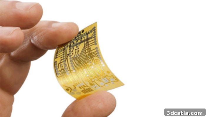
Nano Dimension’s precision 3D printed PCB prototype produced on the DragonFly Pro | Credits: Nano Dimension
The evolution of 3D printing in electronics is highly likely to mirror the adoption patterns seen in other industries where the technology has matured. As the underlying technologies continue to advance, and as more innovative players enter the market, the 3D printing of electronics is expected to transition from being primarily a rapid prototyping tool to a viable and efficient mass production process. To illustrate this potential for scalability, Optomec, another leading company in this segment of additive manufacturing, highlights the impressive capabilities of its Aerosol Jet technology. They report that their system is capable of 3D printing 5,000 integrated circuits, each sized between 25 to 50 µm, per hour. Furthermore, they emphasize that this production rate can be scaled up to an astounding 10,000 circuits per hour with the integration of an additional print nozzle. These figures are a clear indication that companies are not only developing highly precise micro 3D printing solutions but are also building in the capacity for high-volume production, signaling a transformative future for electronics manufacturing.
Other Diverse Applications
Beyond the electronics sector, the ability to precisely print structures at such incredibly small scales opens up a cascade of benefits and applications across various other fields. Numerous innovative startups, including Microfabrica, Nanoscribe, Boston Micro Fabrication, and MicroLight3D, have successfully developed micro-technologies that are being actively utilized to produce highly specialized medical devices. In the critical field of medicine, a paramount concern for medical professionals is to minimize collateral tissue damage during surgical procedures and interventions. Therefore, the continuous miniaturization of medical devices, ranging from surgical tools to diagnostic probes, is of utmost importance. In the medical sector, Nanoscribe further illustrates the power of their 2PP technology by enabling users to fabricate complex 3D scaffolds. These intricate biomimetic structures provide ideal environments for researchers to meticulously study cell growth, migration patterns, and the differentiation of stem cells, paving the way for advancements in regenerative medicine and tissue engineering. Additionally, Nanoscribe’s 2PP technology is being applied to a diverse array of other applications, including the creation of high-precision refractive, diffractive, and micro-optical elements for advanced imaging and sensing systems.
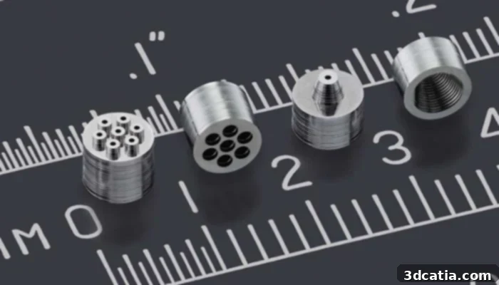
3D printed tools showcasing micrometer precision using metal micro 3D printing | Credits: Microfabrica
The Future Landscape of Microscale Additive Manufacturing
Looking ahead, the future implications of microscale 3D printing are vast and promising, poised to introduce disruptive innovations across multiple industries. Possible applications envision a world where wearable or embedded sensors, fabricated with exceptional precision, continuously monitor health parameters in real-time, offering unprecedented insights into personal well-being. Furthermore, 3D printed sensors could be seamlessly integrated into contact lenses, enabling advanced augmented reality (AR) applications that overlay digital information onto our natural vision. Beyond these, the widespread integration of 3D printed embedded electronics is anticipated in an array of everyday objects, from sophisticated smartphones to autonomous vehicles. This integration promises to add new levels of functionality, enhance user experiences, and contribute significantly to making these products lighter and more energy-efficient. Despite this exciting potential, current limitations primarily revolve around the software capabilities required to develop and optimize intricate models for such minute manufacturing scales. Additionally, there is an ongoing and crucial need to expand the palette of available materials suitable for these ultra-high-resolution printing processes, which will further unlock new applications and functionalities.
In conclusion, it becomes abundantly clear that the broader adoption of micro 3D printing will inevitably encounter hurdles similar to those faced by other additive manufacturing technologies during their growth phases. John Kawola, CEO of Boston Micro Fabrication, offers valuable perspective on this, stating: “We don’t believe the challenges of wider adoption of microscale 3D printing are any different from the challenges of wider adoption of 3D printing in general. 3D printing across all sizes will continue to be invaluable for engineering and design prototyping, enabling faster iteration and innovation. Microscale 3D printing, however, introduces some entirely new tools to engineers who previously lacked effective methods for prototyping at that extremely small scale. Furthermore, the conventional production of microscale parts is typically quite expensive and complex, which significantly increases the value proposition of considering 3D printing for the direct production of high-performance end-use parts, offering both cost savings and design freedom.” This perspective underscores that while challenges exist, the unique advantages and capabilities of microscale 3D printing make it an indispensable technology for future innovation and manufacturing efficiency.
What do you envision microscale 3D printing contributing to the additive manufacturing industry in the coming years? We invite you to share your thoughts and predictions in a comment below or connect with us on our Facebook and Twitter pages! Don’t forget to sign up for our free weekly Newsletter to receive all the latest news and insights in 3D printing delivered directly to your inbox!