News
University Researchers Create New Method to Print Copper on Fabric for Wearable Electronics
Recently, researchers from the Department of Electrical Engineering at the University of South Florida (USF) received a patent and official grant of $369,574 from the National Science Foundation (NSF). This will be used for the development of a method to…
- 3 min read
- News
- Six more stories
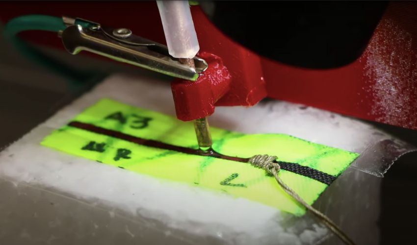
Recently, researchers from the Department of Electrical Engineering at the University of South Florida (USF) received a patent and official grant of $369,574 from the National Science Foundation (NSF). This will be used for the development of a method to 3D print copper directly on fabric. The new electrochemical process marks a new milestone in the advancement of wearable electronics.
In this day and age, electronic gadgets have developed to a level that no one would have imagined a few decades ago. Long gone are the days of chunky devices that served a single purpose only. Nowadays we have smartwatches, multifunctional headphones, and even wearable computer glasses are available, and it is not inconceivable that the possibility of having wearable electronics that are embedded into clothing might be just around the corner. In an attempt to further advance such technologies, Department of Electrical Engineering Associate Professor Arash Takshi and USF Research & Innovation Interim Vice President and Professor Sylvia Thomas have developed a new method called hydrogen evolution assisted (HEA) electroplating that makes it possible to print copper directly on fabrics, opening the door to an abundance of technological innovations.
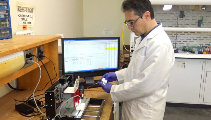
Professor Arash Takshi at Work (photo credits: USF)
Creating Wearable Electronics with Copper 3D Printing
The new process consists of two steps of additive manufacturing. First, laser printing technology is used to apply a conductive template to the fabric. In the process, the fabric is carbonized, which enhances its stability and makes it more durable. In the next step, electroplate copper is used to produce a continuous copper pattern that forms the circuit layout of the electronic component on the fabric. The specially designed nozzle, that is mounted on a 3D printing device, enables localized electroplating and makes it possible to make the copper grow in the junctions between the electronic components’ terminals and the circuit printed layout, and solder them at room temperature. The main difference between the newly introduced method and the way it has been done in the past is that Takshi and Thomas’ method increased the voltage applied during the process, which ultimately results in the water electrolysis at the same time that copper grows, making the process faster and enhancing the mechanical stability of the printed structure.
More from the desk
Six other notes from the rest of the bench.
 ApplicationsHow is Additive Manufacturing Being Adopted in Defense?When it comes to the military, flexibility and innovation are key in ensuring the success of operations in all corners of the globe. Indeed, when we think of military personnel one of the underlying characteristics of their actions is rapidity,…
 NewsProject uses 3D printing to supersize and study pollenIn fields as far-ranging as medical and aerospace engineering, 3D printing has applications that can help students and professionals understand complicated concepts. For example, in the medical sector, exact anatomical models of patients’ organs are 3D printed to plan and&h
 NewsAre 3D Printer Shipments Back to Pre-COVID Levels?When the pandemic shut down the world last year, a number of industries were severely impacted. However, 3D printing proved to be more robust than many others. That being said, a few studies have shown that though it did not…
 ApplicationsBMW M Visionary Materials Seat Wins Sustainability Prize Thanks to 3D PrintingThe automotive industry is steadily moving towards greater sustainability and 3D printing is playing a crucial role in this transition. This is because additive manufacturing enables companies to produce more environmentally friendly, lighter and more efficient components. This i
 NewsNew Balance and Formlabs continue to leverage TripleCell platformWe told you at the beginning of July about the 3D printing platform that had just been launched by New Balance and Formlabs – the TripleCell platform. At the time, the companies announced that this platform would be used to…
 Printers3Dnatives Lab: Testing the BQ Witbox Go! 3D printerThe Spanish manufacturer BQ, which is responsible for a wide range of 3D printers and is one of the leading European manufacturers, with the Plug & Play models Witbox 1 and Witbox 2, recognisable by their volume of printing, as well as the machines…