
Revolutionizing Space Exploration: The Dawn of 3D Printed Electronics in Space
In recent years, the landscape of manufacturing has been profoundly reshaped by the rapid advancements in additive manufacturing, more commonly known as 3D printing. This transformative technology has surged in popularity across an astonishing array of industries, primarily due to its unparalleled ability to facilitate customization, inspire innovative designs, and deliver components with significantly improved performance characteristics. From medical devices to automotive parts, and from consumer goods to intricate aerospace components, 3D printing’s widespread adoption underscores its versatility and strategic importance. Among the many sectors eagerly exploring and harnessing the profound potential of 3D printing, space exploration consistently stands out as a pioneering frontier, driving and benefiting from the cutting edge of this technology.
At the forefront of this celestial push is NASA, the world-renowned space agency, which has consistently dedicated substantial resources to researching, developing, and deploying groundbreaking additive manufacturing technologies for a multitude of space missions. Their long-term vision involves enabling more complex, lighter, and more efficient spacecraft, alongside facilitating in-space manufacturing capabilities. In a testament to their unwavering commitment to innovation, NASA engineers, in close collaboration with leading academic institutions, recently marked a truly significant milestone. They successfully conducted tests of hybrid printed electronic circuits near the very edge of space, a groundbreaking achievement that signals a crucial evolutionary leap for 3D printing technology and its applications beyond Earth’s atmosphere.
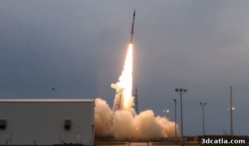
This historic test took place during the Suborbital Technology Experiment Carrier-9 (SubTEC-9) mission, which commenced with a successful launch from NASA’s Wallops Flight Facility. The primary objective of this mission was to rigorously evaluate the viability and performance of these printed circuits under the extreme and unpredictable conditions found in space. The sounding rocket, a critical component of suborbital flight tests, majestically ascended to an impressive altitude of approximately 174 kilometers (equivalent to 108 miles). During its relatively brief but incredibly valuable flight, the mission meticulously collected crucial data regarding the functionality and durability of the printed electronics. This highly successful endeavor conclusively demonstrated the immense potential of 3D printed electronic circuits, paving the way for the development of future spacecraft that are not only smaller and lighter but also boast significantly enhanced capabilities, thereby opening entirely new horizons and opportunities for advanced space exploration and scientific discovery.
One of the most compelling advantages of this innovative technology was eloquently articulated by Dr. Margaret Samuels, an accomplished electronics engineer at NASA’s Goddard Space Flight Center and a co-leader of the groundbreaking SubTEC-9 experiment. Dr. Samuels highlighted, “The uniqueness of this technology is being able to print a sensor actually where you need it.” This statement underscores a paradigm shift in how electronic components can be integrated into spacecraft. Traditional electronics manufacturing often involves pre-fabricated boards that must then be fitted into a given design, sometimes requiring compromises. With 3D printed electronics, sensors and circuits can be directly integrated onto or within structural components, conforming precisely to complex geometries and maximizing functional efficiency. She further elaborated on the practical benefits, stating, “The big benefit is that it’s a space saver. We can print on 3-dimensional surfaces with traces of about 30 microns – half the width of a human hair – or smaller between components. It could provide other benefits for antennas and radio frequency applications.” This level of miniaturization and precision is critical for space missions where every gram of mass and every cubic millimeter of volume carries significant cost and performance implications.
3D Printed Circuits: A Leap Forward in Space Technology and Design
The innovative methodology presented by 3D printed electronics transcends mere space-saving. It enables the creation of incredibly intricate and sophisticated circuits with conductive traces as fine as 30 microns. To put this into perspective, this dimension is half the average thickness of a human hair, representing an extraordinary level of precision previously unattainable through conventional manufacturing techniques for integrated electronics in complex, non-planar forms. This unprecedented capability allows for a dense packing of components and the realization of highly compact, multi-functional systems. Furthermore, the inherent flexibility of additive manufacturing means these circuits can be printed directly onto or within three-dimensional surfaces, eliminating the need for bulky enclosures or extensive wiring harnesses. This direct integration streamlines design, reduces weight, and minimizes potential points of failure, all critical factors for mission success in the unforgiving environment of space.
The applications of this groundbreaking technology extend far beyond simple sensors. As Dr. Samuels suggested, its utility in enhancing antennas and various radio frequency (RF) components is particularly promising. Imagine antennas that are not rigid structures but are seamlessly integrated into the spacecraft’s skin, or RF modules that are lightweight and precisely tuned due to their custom-printed geometries. These possibilities translate directly into significant improvements in spacecraft design, leading to lighter, more agile, and more capable platforms. The ability to customize and integrate electronics directly into the structural elements of a spacecraft offers a pathway to unprecedented levels of system integration, where form and function are harmoniously merged, ultimately boosting overall performance and expanding the scope of what future space missions can achieve.
The resounding success of the SubTEC-9 mission was not an isolated achievement but a direct result of a powerful collaborative effort between NASA’s Goddard Space Flight Center and the University of Maryland’s Laboratory for Physical Sciences (LPS). This partnership exemplified the synergistic benefits of bringing together diverse expertise from government agencies and academic research institutions. Working in unison, these dedicated experts meticulously developed not only the sophisticated humidity-sensing printing ink but also the intricate circuits themselves. This achievement underscores the vital importance of inter-organizational cooperation in driving forward cutting-edge technologies. The blend of NASA’s mission-critical requirements and deep understanding of space environments with the University of Maryland’s advanced material science and fabrication research proved to be an unstoppable force, demonstrating how shared goals and complementary skills can accelerate technological breakthroughs that have far-reaching implications for scientific exploration and engineering innovation.
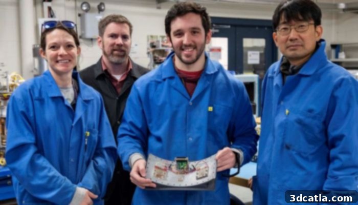
NASA and the University of Maryland’s Laboratory for Physical Sciences (LPS) engineering team showcased their printed electronics test assembly with a curved metal plate at a NASA Wallops Flight Facility lab before SubTEC-9’s historic technology test flight in April 2023. This marked the first flight of hybrid printed electronic circuits in space. (Credit: NASA/Berit Bland)
The successful deployment and testing of these hybrid printed electronic circuits aboard the SubTEC-9 mission mark not an end, but a promising beginning, opening new avenues for further innovation and application. Buoyed by this triumph, engineers are already actively exploring the transformative potential of printing various types of sensors directly onto or within a spacecraft’s interior. One particularly compelling application involves the integration of temperature sensors throughout the entire structure of a spacecraft. This capability would allow for unprecedented, real-time thermal mapping, enabling engineers to gain a far more detailed and nuanced understanding of the complex effects of heating and cooling cycles during critical space missions. Such data is invaluable, especially when spacecraft are maneuvering near celestial bodies like the Sun, where extreme temperature fluctuations can severely impact sensitive onboard equipment. Enhanced thermal monitoring through integrated printed sensors could lead to more robust designs, better thermal management systems, and ultimately, extended mission lifetimes and improved reliability.
As NASA and its dedicated partners continue their relentless efforts to refine and significantly expand the capabilities of 3D printing in the realm of advanced electronics, the global scientific community watches with eager anticipation. The future possibilities that this technology holds for the trajectory of space exploration are nothing short of immense and transformative. Beyond improved functionality in critical antenna connections and the development of more efficient radio frequency components, the potential applications are truly extensive and far-reaching. Imagine mission-specific X-ray instruments that are lighter, more compact, and exquisitely tailored for specific astronomical observations, or integrated structural health monitoring systems that can detect micro-fractures or anomalies in real-time, greatly enhancing safety and extending operational lifespans. Furthermore, the ability to print circuitry in situ could revolutionize CubeSat and small satellite development, allowing for more payload capacity and complex functionality within constrained volumes. This technology paves the way for a new era of space exploration, characterized by unprecedented levels of miniaturization, integration, and performance across all mission profiles, from orbital mechanics to deep-space probes. For those seeking additional in-depth information, the original source can be found HERE.
What are your thoughts on the groundbreaking advancements in 3D printed circuits for space applications? Do you envision other transformative uses for this technology? We invite you to share your insights and comments below, or engage with us on our LinkedIn, Facebook, and Twitter pages! Don’t miss out on the latest developments in additive manufacturing – be sure to sign up for our free weekly Newsletter here, delivering the freshest 3D printing news straight to your inbox! You can also explore all our insightful videos and content on our dedicated YouTube channel.
*All photo credits: NASA