
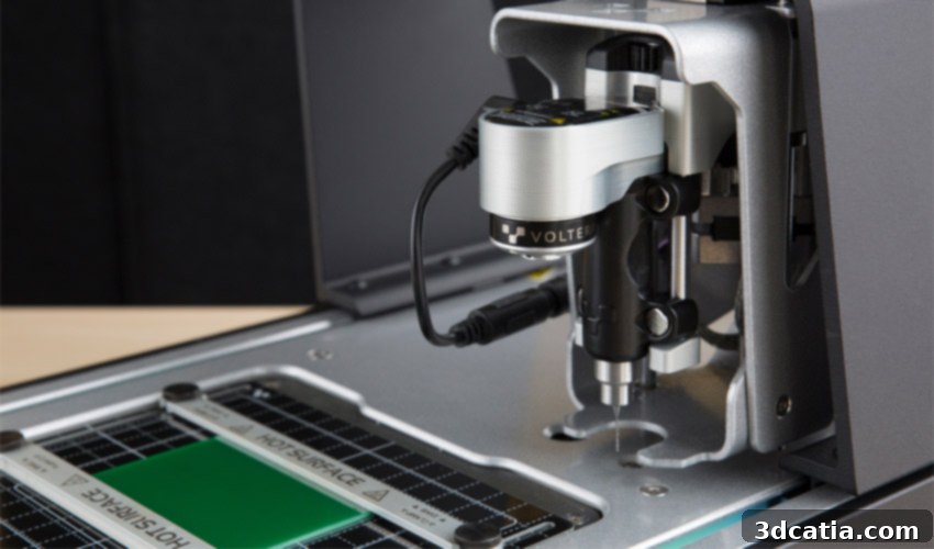
Voltera: Revolutionizing Electronics Prototyping and On-Demand PCB Manufacturing with Additive 3D Printing
Additive manufacturing, commonly known as 3D printing, has profoundly transformed numerous industries, yet its impactful role within the electronics sector is often less discussed. Here, this innovative technology, specifically known as micro 3D printing or additive electronics, empowers engineers to design and produce components that are significantly smaller, finer, and more precise than what traditional production methods typically allow. This capability translates directly into improved performance, enhanced functionality, and crucial miniaturization for electronic devices across a spectrum of applications. While traditionally confined to early-stage prototyping, leading to faster iterations and reduced development cycles, a new wave of innovation is pushing the boundaries beyond mere conceptualization. This is precisely where Voltera, an pioneering startup, is making its mark, focusing on leveraging additive manufacturing to create functional printed circuits, extending its utility far beyond the initial prototyping phase. By developing a sophisticated yet accessible machine for in-house circuit production, Voltera aims to fundamentally revolutionize the electronics industry, democratizing access to advanced PCB (Printed Circuit Board) fabrication. We recently had the opportunity to speak with Alroy Almeida, one of Voltera’s visionary co-founders, to delve deeper into the capabilities of their groundbreaking 3D printer and to understand his comprehensive outlook on the future of this rapidly evolving sector.
3DN: Can you introduce yourself and tell us about your relationship with 3D printing and additive manufacturing?
My name is Alroy Almeida, and I am one of the co-founders of Voltera. My journey with 3D printing stretches back over a decade, primarily involving the creation of various mechanical components for diverse projects. At Voltera, prototyping forms a significant part of our daily operations. Initially, we relied on filament-based printers for our mechanical prototypes, but over the last few years, we’ve transitioned to Stereolithography (SLA) technology, utilizing both our own machines and specialized print shops for more intricate designs. While I continue to closely monitor the advancements and trends within the broader 3D printing landscape, my primary focus and intrigue lie squarely with Additive Electronics (AE). Given Voltera’s core mission as an Additive Electronics company, I am particularly fascinated by the current state-of-the-art and the promising future developments in AE technologies, which are poised to redefine how we design, develop, and manufacture electronic systems.

Alroy Almeida (right) with part of the Voltera team.
3DN: What inspired you to launch Voltera and tackle the challenges in electronics manufacturing?
The inception of Voltera dates back to 2012 when my co-founders and I recognized a glaring disparity in the prototyping landscape. While mechanical 3D printers had become incredibly versatile and accessible tools for rapid iteration of physical components, a comparable solution for electronics engineers simply didn’t exist. This absence created significant bottlenecks during the critical early stages of product development. Engineers were routinely forced to endure weeks of waiting for prototype Printed Circuit Boards (PCBs) to arrive from distant factories, or had to pay exorbitant fees to expedite delivery – a cost that often proved prohibitive for startups and smaller teams. These delays and high costs made electronics the primary bottleneck for numerous companies striving to bring innovative products to market efficiently. We experienced this firsthand and learned these harsh lessons while designing electronics in various professional settings. My personal background was rooted in industrial electronics, specifically ruggedized communications designed for factories and other challenging environments, alongside some development work on medical devices. My business partners, on the other hand, brought extensive expertise in automation, electronic design automation (EDA), and cutting-edge materials research. This collective experience highlighted a clear and pressing market need.
Armed with our respective Mechatronics and Nanotechnology Engineering degrees, we decided to channel our skills into creating a circuit printer. Initially, our motivation was to “scratch our own itch” – to develop a solution that would solve our personal frustrations with PCB prototyping, primarily to see if such a feat was even possible. However, it wasn’t long before former colleagues and friends began expressing keen interest in our project. This external validation transformed our perspective, shifting our focus from a mere internal project to developing a full-fledged product with the potential to empower countless electronics engineers. This marked the true beginning of Voltera, driven by a passion to democratize access to rapid, on-demand PCB fabrication.
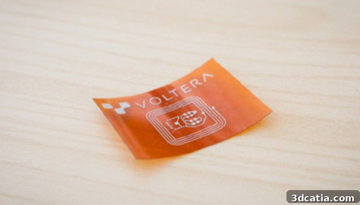
A sophisticated 3D printed circuit board created by Voltera’s technology.
3DN: Could you elaborate on the functionality and operational workflow of the Voltera V-One circuit printer?
Before delving into the intricate printing process of the V-One, it’s crucial to understand how a circuit design transitions from a concept into a printable file. The V-One utilizes our proprietary CAM software, which is designed to accept Gerber files. Gerber files are the universally recognized standard format for PCB layout data, meaning they can be seamlessly exported from virtually any CAD (Computer-Aided Design) tool that engineers are already familiar with and using. This approach ensures complete CAD tool agnosticism, preserving your existing design workflow without disruption. Once the Gerber files are loaded into our software, they are intelligently converted into precise tool paths for the V-One. Following this conversion, the machine undergoes an automated calibration sequence, ensuring optimal accuracy and readiness to commence the circuit board creation process.
The V-One is engineered to facilitate the creation of double-sided boards through a streamlined, multi-step process:
1) The process begins with the precise drilling of holes for vias (vertical interconnect access) and through-hole components, ensuring accurate alignment for electrical connections between layers and component mounting.
2) Next, the V-One meticulously prints the top layer of the circuit using conductive ink. This layer is then thermally cured within the machine, solidifying the conductive traces and preparing the board for subsequent steps.
3) Following the top layer, the machine proceeds to print the bottom layer of the circuit. Similar to the top layer, this layer also undergoes a crucial thermal curing process to ensure durability and conductivity.
4) Once both layers are printed and cured, PCB rivets are quickly and easily added manually to establish robust electrical connections through the vias, linking the top and bottom layers.
5) The V-One then precisely dispenses solder paste onto the designated pads, preparing the board for component attachment with exceptional accuracy.
6) Finally, components are manually placed onto the solder paste. The machine then performs a controlled reflow soldering process, melting the solder paste to securely bond the components to the board, completing the assembly.
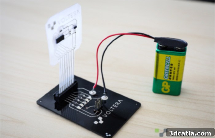
For those interested in the granular details, the full specifications for the V-One printer are readily available. Key highlights include its capability to produce double-sided circuits with an impressive 0.65mm pin-to-pin pitch, accommodating passive components down to the compact 0402 size, and achieving an 8mil (thousandths of an inch) trace and space resolution. The effective print area for circuit fabrication is a generous 128mm × 116mm. The machine is designed for global accessibility, offered with both European and North American plug configurations and voltage compatibility. The conductive ink, central to creating the circuit traces, is silver-based. Despite its silver content, it is remarkably cost-effective; each $99 ink cartridge possesses the capacity to print dozens of circuit boards, making in-house production economically viable. Similarly, a $49 cartridge of solder paste can cover thousands of pads, further reducing per-board costs. While the V-One is primarily designed to print on standard FR4 and FR1 fiberglass boards, its versatility extends to a wide array of alternative substrates, including glass, paper, Polyimide (PI), PET, and various other flexible materials, opening up possibilities for innovative applications. The integrated 550W heater is a critical component, performing both the thermal curing of the conductive ink and the reflow of the solder paste, utilizing both standard and customizable heating profiles to ensure optimal results for different materials and circuit complexities.
3DN: What is Voltera’s overarching mission, and what impact has your technology had globally?
Our mission at Voltera is fundamentally about empowerment: empowering innovators, educators, and researchers worldwide to accelerate hardware development. We are incredibly proud to report that we currently have thousands of V-One machines deployed in over 65 countries across the globe. These machines are being utilized by a diverse spectrum of users, from hardware businesses of all sizes striving to bring groundbreaking ideas to market faster, to academic and government researchers pushing the boundaries of scientific discovery with breakthrough technologies. Furthermore, the V-One plays a crucial role in educational institutions – high schools, colleges, and universities – by providing hands-on experience that trains the next generation of engineers and technologists. The applications are incredibly varied and impactful, encompassing the development of advanced robotics, sophisticated satellite components, life-saving medical technologies, critical automotive parts, and dozens of other innovative applications, each benefiting from the ability to rapidly iterate and test custom electronics.
Our current strategic goal is to continuously enhance the capabilities we offer our customers and to help new users integrate rapid hardware development into their workflows even more seamlessly. This mission has become particularly pertinent in recent times, especially during and after 2020. The global pandemic imposed unprecedented challenges, causing significant disruptions, loss of time, and depletion of resources for countless businesses. In such a demanding environment, hardware developers were, and still are, being asked to achieve more with fewer resources, often needing to meet stringent deadlines while working remotely. The V-One directly addresses these challenges.

Thanks to its compact size, the Voltera V-One machine easily adapts to various work environments, from labs to home offices.
Designed with versatility in mind, the V-One is compact enough to sit comfortably on a standard workbench, yet its small footprint allows it to feel perfectly at home on a dining table or within a dedicated home office setup. This portability is revolutionizing hardware development processes. The ability to email design files – Gerber files – to a colleague across the city or even across the globe, and have them print a fully functional circuit board within an hour, fundamentally changes the paradigm. It eliminates the previous reliance on distant factories, the associated lengthy lead times, and the logistical complexities of shipping parts back and forth. We’ve witnessed firsthand the profound impact of this capability, with customers working on critical projects such as respirators and advanced COVID-19 testing devices. Having a “mini PCB factory” directly on their desk allowed them to significantly accelerate their development cycles, proving indispensable during moments of urgent global need. This embodies Voltera’s commitment to fostering innovation and resilience in hardware design.
3DN: What are Voltera’s future projects, and where do you envision the company in the next five years?
While the majority of V-One machines are currently utilized by businesses for commercial and industrial applications, we see an immense and largely untapped opportunity to expand our collaboration with educators. The V-One was originally engineered for professional use, emphasizing precision and reliability, yet its intuitive design and ease of use have made it incredibly accessible to university and even high school students around the world. We believe the V-One is poised to play a transformative role in hands-on electronics education. While a strong theoretical and mathematical understanding of electronics is undeniably important, it is the tangible, creative component – the act of designing, fabricating, and testing a physical circuit – that truly inspires students and motivates them to pursue rewarding careers in product development and engineering. By providing direct access to PCB manufacturing, we aim to bridge the gap between theory and practical application, fostering a deeper understanding and passion for electronics.
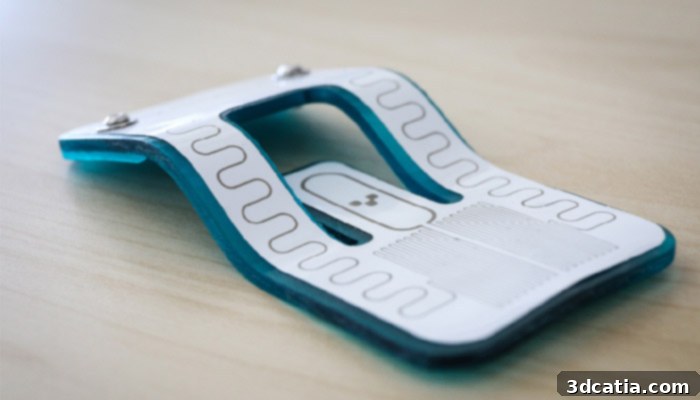
Our product roadmap is dynamically and significantly influenced by our vibrant user community. The next generation of machines currently under development is a direct response to how our users are creatively “hacking” the V-One to explore and create more exotic forms of electronics. This includes circuits that possess remarkable flexibility or stretchability, designs that can conform precisely to the contours of their enclosures, or those that leverage novel substrates for critical weight-savings and advanced form-factor manipulation. These cutting-edge additive electronics applications are pushing the boundaries of what’s possible in device design, enabling integration into previously impossible spaces or materials.
Presently, these advanced technologies are primarily confined to a very small subset of pioneering electronics designers. This limited adoption is largely due to two key factors: the prototyping and manufacturing processes for these exotic electronics are unfamiliar to most, and there’s a serious lack of comprehensive educational resources and established design methodologies for these specialized use cases. Voltera is deeply committed to changing this landscape. We have a substantial amount of work underway to demystify these processes, provide the necessary tools, and develop educational content that will make flexible, stretchable, and conformal electronics accessible to a much broader audience. If you are interested in learning more about these exciting developments, or if you simply wish to share your own experiences with the challenges in this area, please feel free to contact me directly. You can also discover more comprehensive information and stay updated on Voltera’s latest innovations by visiting our official website.
What are your thoughts on Voltera’s pioneering activities in the electronics sector and the future of additive manufacturing for PCBs? We invite you to share your insights in a comment down below or join the conversation on our Facebook and Twitter pages! Don’t forget to subscribe to our free weekly Newsletter to receive all the latest news and innovations in 3D printing directly in your inbox!