
Revolutionizing Electronics: The Future of 3D Printed PCBs with Nano Dimension’s DragonFly 2020
In the rapidly evolving landscape of advanced manufacturing, a pioneering Israeli company, Nano Dimension, stands at the forefront of innovation. Established in 2012, Nano Dimension has specialized in the intricate fields of nanotechnology and additive manufacturing, fundamentally transforming the way electronics are designed and produced. Their groundbreaking work centers on the development of unique inkjet inks, meticulously engineered with nanoparticles. These advanced inks are the cornerstone of their proprietary 3D printing system, the DragonFly 2020, which is specifically designed for the ultra-rapid production of high-performance printed circuit boards (PCBs).
The DragonFly 2020 system empowers engineers and designers to create complex electronic circuits that can feature multiple conductive layers, offering unparalleled flexibility in design – whether the application demands rigid or flexible substrates. This additive manufacturing approach dramatically accelerates production cycles, moving from conceptualization to functional prototype in a fraction of the time traditionally required. To delve deeper into this innovative technology and its far-reaching implications, we recently had the opportunity to speak with Nano Dimension’s Chief Business Officer, Simon Fried, who provided invaluable insights into their vision and achievements.
3DN: Could you please present Nano Dimension and elaborate on the transformative work that you do?
My name is Simon Fried, and I serve as the CBO of Nano Dimension. At Nano Dimension, our core mission has been to converge three critical technological domains: additive manufacturing, advanced nanotechnology, and the dynamic world of electronics. We have seamlessly integrated these fields through our flagship product, the DragonFly 2020 3D printer. The DragonFly system represents a pinnacle of precision engineering, linking the unparalleled accuracy of our inkjet 3D printing technology with our sophisticated nanoparticle inks and intelligent software. This synergistic combination enables the ultra-rapid prototyping of highly complex, multilayer, and professional-grade printed circuit boards (PCBs), a capability that was previously unimaginable within typical R&D environments.
What truly excites us about our technology is the profound impact this 3D printing platform has on the design and engineering process. It grants designers and engineers the unprecedented ability to print functional electronic prototypes in-house, often within a matter of hours. This capability dramatically compresses traditional product design and testing cycles from weeks or months down to mere days. The direct consequence of this accelerated workflow is a significant strengthening of a company’s in-house innovation capabilities, fostering an environment where iterative design and experimentation thrive. Furthermore, by keeping the prototyping process entirely in-house, our technology provides enhanced R&D IP (Intellectual Property) security, a crucial advantage in today’s competitive technological landscape.

Simon Fried, The CBO of Nano Dimension
3DN: Can you describe the core technology utilized in your 3D printer, and what makes your specialized inks so innovative?
The DragonFly 2020 itself leverages a robust and proven technology similar to that developed by Stratasys’ PolyJet systems. This method allows us to precisely jet multiple materials simultaneously, enabling the direct 3D printing of complex multilayer circuit boards within hours. This rapid turnaround is a game-changer for product development. Our system is uniquely capable of producing metal and polymer combination prints, which are absolutely ideal for the intricate demands of PCB and electronic prototyping. Once the additive printing process is complete, auxiliary electronic components, such as transistors, resistors, capacitors, and integrated circuits, can then be seamlessly integrated onto or into the 3D printed substrate. This crucial step allows the user to perform comprehensive functional testing of the finished PCB prototype, ensuring its performance meets specifications before committing to costly traditional manufacturing.
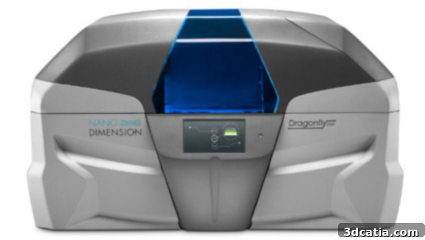
The DragonFly 2020 3D Printer
The true innovation, however, lies in our in-house developed nanoparticle inks. We utilize AGCite nanoparticle conductive silver inks alongside our advanced dielectric inks to construct these intricate PCBs. Our team of expert scientists has perfected methods to produce incredibly pure silver particles, ranging in size from a mere 10 to 100 nanometers. This precise control over the nanoparticle manufacturing process is critical. By meticulously controlling the size, shape, and dispersion of these silver nanoparticles within the ink, we can achieve optimal levels of electrical conductivity, mechanical flexibility, and robust adhesion to the substrate. This ensures that the printed traces are not only highly efficient but also durable and capable of performing under various conditions.
Our dielectric ink is equally remarkable and is a testament to our material science expertise. It was engineered specifically as a functional material, possessing distinct properties essential for its role. Its primary function is to effectively insulate the conductive ink layers, thereby enabling the intricate layering required for a sophisticated circuit board structure. Furthermore, this proprietary dielectric ink boasts exceptionally high thermal stability, a vital characteristic for electronics. It can withstand very high temperatures, up to 350° C (662° F), without compromising its insulating properties. This thermal resilience is crucial for the reliability and longevity of the printed electronic components, particularly in demanding applications where heat dissipation and operational stability are paramount.
3DN: What are the fundamental benefits that 3D printing brings to the production of electronics, particularly for printed circuit boards?
The ability to seamlessly merge printed electronics with the transformative power of 3D printing is catalyzing unprecedented innovation across both domains. Traditionally, the process of obtaining a prototype for a complex 10-layer PCB could entail a two-week turnaround time, sometimes even longer, often involving multiple external suppliers. This lengthy and costly cycle frequently forces engineers to adopt a highly conservative approach during the design process, as any misstep or design flaw can lead to significant financial costs, extended delays, and project setbacks. The inherent risks associated with traditional PCB manufacturing stifle creativity and limit exploratory design.
With the advent of 3D printed electronics, this paradigm is fundamentally shifting. Engineers are liberated from the constraints of conventional manufacturing, empowering them to embrace a more innovative and agile design methodology. They gain unparalleled flexibility throughout the entire development process, enabling rapid iteration, immediate testing, and design modifications on the fly. This profound change in workflow has a strong and immediate impact on the production of a vast array of consumer technologies and specialized electronic devices. For instance, consider the traditional limitations on how PCBs are designed; 3D printing allows for unprecedented geometric freedom. We are rapidly moving towards a future where we can routinely produce complex three-dimensional coils and even embed entire electronic components directly within the substrate of a device during a single print job. This opens up possibilities for miniaturization, enhanced functionality, and novel form factors that were previously impossible to achieve with conventional planar manufacturing techniques.

A printed circuit created thanks to additive manufacturing
3DN: How do you envision the future evolution and impact of 3D printed electronics?
The ultimate aspiration, often referred to as the ‘holy grail’ of 3D printing, is to possess the capability to print fully functional, customized objects in a single build process. This includes the seamless integration of complex electronic systems directly into the printed object. This ambitious vision is one of our foundational goals, and it’s precisely what we have embarked upon with the development of the DragonFly 2020. Our work is a crucial step towards realizing this future, demonstrating the potential for integrated functional prototypes.
Looking ahead, we anticipate that 3D printed electronics will evolve significantly through the use of an even broader spectrum of materials. This will extend beyond current conductive and dielectric inks to include semiconductor materials, specialized polymers, and perhaps even optical materials, all printable within a single system. Furthermore, we expect a dramatic increase in the flexibility with which these diverse materials can be combined, allowing for multi-functional structures and embedded capabilities far beyond what is currently achievable. This expansion of material libraries and combination possibilities will unlock entirely new applications and product categories.
Concurrently, we are projecting a continued and robust growth in the sophistication and accessibility of 3D printing systems for electronics. This growth will be driven by continuous improvements aimed at overcoming some of the sector’s most persistent challenges: namely, speed, scale, and precision. Future systems will feature significantly faster print speeds, enabling higher throughput and greater efficiency for production. We will also see an increase in the scale of these systems, allowing for larger components or the simultaneous production of multiple items. Critically, precision will reach unprecedented levels, facilitating the creation of even more intricate and miniaturized electronic structures. These advancements will collectively propel 3D printed electronics from a powerful prototyping tool to a viable, high-volume manufacturing solution, playing a pivotal role in the fourth industrial revolution.

3DN: We recently learned about your launch of a 3D bio-printing subsidiary. Could you share more details about this exciting new venture?
Indeed, this is a very exciting development for Nano Dimension. We firmly believe that by strategically combining our extensive know-how in multi-material 3D printing – a core competency refined through our work with the DragonFly 2020 – with our specialized expertise in nano-chemistry, we are uniquely positioned to provide significant added value to the promising and rapidly expanding field of bio-printing. Our ambition within this new subsidiary is to leverage these synergistic capabilities to create highly complex biological structures, pushing the boundaries of what is currently possible in regenerative medicine and pharmaceutical research.
This dedicated subsidiary allows us to channel our efforts and focus solely on the intricate challenges and immense potential of 3D bio-printing. We have already made significant strides, demonstrating a successful proof of concept by performing 3D bio-printing of functional tissue incorporating live stem cells. This critical milestone validates our approach and showcases the feasibility of our technology for biological applications. Furthermore, to protect our innovative work and secure our position in this nascent field, we have diligently filed a comprehensive patent application for our advanced bio-printing technology, ensuring that our intellectual property is safeguarded as we continue to advance this transformative initiative.
3DN: Do you have any final remarks or insights you would like to share with our readers?
Absolutely. The DragonFly 2020 3D printer is currently undergoing rigorous evaluation by a diverse group of beta customers across a variety of demanding industries. These include the defense sector, where rapid prototyping and secure in-house manufacturing are critical; the consumer goods industry, which benefits from accelerated product development cycles and innovative designs; technology companies serving the finance industry, requiring specialized and high-security hardware; and the medical devices sector, where precision, miniaturization, and customization are paramount. The invaluable feedback and insights gathered from these key industries are instrumental in refining our system and preparing it for broader adoption.
We are thrilled to announce that the DragonFly 2020 system is scheduled for its highly anticipated commercial release later this year. This global rollout will strategically target key manufacturing and technology hubs across the United States, Europe, and Asia. This broad market introduction underscores our confidence in the DragonFly 2020’s ability to fundamentally transform electronics development workflows worldwide. We invite everyone interested in the future of electronics and additive manufacturing to follow our journey and witness the incredible potential of 3D printed PCBs.
For more comprehensive information regarding Nano Dimension’s cutting-edge technology and vision, please visit our official website, which can be found here. Additionally, we encourage you to watch our engaging interview with Simon Fried himself, recorded live at Solidworks World 2017, where he shares further insights into our innovations:
We’d love to hear your thoughts! What do you envision for the future of 3D printing within the electronics industry? Share your perspectives and ideas in the comment section below!
And don’t forget to connect with us and stay updated on our latest news by adding us on Facebook and following us on Twitter!