
Unlocking Innovation: The Pivotal Role of a Materials Engineer in Advanced 3D Printing
Welcome back to our #Working3D series, a dedicated exploration into the diverse and fascinating professions within the additive manufacturing industry. This installment shines a spotlight on a truly fundamental aspect: the materials. After all, without the right materials, there can be no successful print – no intricate components, no functional prototypes, and no groundbreaking innovations. We delve into the critical work of the individuals who conceive, develop, and refine the very substances that bring 3D designs to life – the materials engineers. What does it truly mean to be an engineer responsible for cutting-edge materials in additive manufacturing? What specific blend of skills, expertise, and innovative thinking do they contribute to enable the creation and versatile application of 3D printing materials across an astonishing array of industries and research fields? To unravel these compelling questions, we sat down with Markus Lunzer, the esteemed Team Leader for Materials & Application at the innovative Viennese company UpNano GmbH. Mr. Lunzer generously shared profound insights into the essential qualifications for a materials engineer in this dynamic sector and offered a detailed glimpse into his daily professional life, highlighting the intricate dance between material science and practical application in high-resolution 3D printing.
3DN: Could you please introduce yourself and provide an overview of your professional journey?

My name is Markus Lunzer, and my academic foundation was meticulously built at the Vienna University of Technology (TU Wien), where I pursued a degree in technical chemistry. My studies provided a strong emphasis on synthetic chemistry, a field that comprehensively explores how to design, create, and manipulate novel substances at the molecular level. This deep understanding of chemical synthesis lays the groundwork for innovative material development. For my doctoral dissertation, I immersed myself in the fascinating world of photopolymerization, specifically focusing on the development of light-cleavable hydrogels. Photopolymerization is a process where light energy triggers chemical reactions to form polymeric materials, offering precise control over material structure. My research explored how these hydrogels – highly water-absorbent polymer networks with significant potential in biomedical applications – could be precisely formed and, crucially, selectively broken down or structured using light. This work was pivotal in understanding light-matter interactions for advanced fabrication. Upon the successful completion of my studies in 2019, I embarked on my professional career in materials development at UpNano GmbH. This company, then a newly established pioneer in the rapidly advancing field of 2-photon 3D printing technology, offered an incredibly exciting opportunity to apply my specialized knowledge in a commercial setting. I quickly became an integral part of their innovative team, contributing to the foundational material science that drives their technology. For the past four years, I have had the distinct privilege of leading the materials and applications team, driving the continuous development and versatile application of groundbreaking materials specifically designed for ultra-high-resolution additive manufacturing. My journey has been a fulfilling blend of academic rigor and industrial innovation.
3DN: How did your path lead you into the dynamic field of additive manufacturing, particularly 2-photon polymerization?
My initial foray into additive manufacturing, particularly 2-photon polymerization (2PP), began quite organically during my master’s thesis research. At that time, I was synthesizing specific molecules, meticulously designed for their structural suitability as highly effective photoinitiators for 2PP. Photoinitiators are crucial components within a photopolymerizable resin; they are chemical compounds that absorb light energy and, in doing so, initiate the polymerization process that transforms a liquid resin into a solid 3D structure. 2PP itself is a remarkably high-resolution 3D printing technology that leverages a pulsed laser to selectively cure minuscule volumes of resin, enabling the creation of incredibly intricate components with features in the sub-micrometer range – far beyond the capabilities of conventional manufacturing. While rigorously testing these newly synthesized molecules on experimental machines available at the university, I experienced a profound realization. The precision, speed (even in its early forms), and inherent potential of this technology were truly astounding. I quickly understood that 2PP was not just a niche academic tool but held immense promise as a transformative manufacturing method with broad industrial implications. This discovery solidified my resolve to deepen my involvement. Consequently, for my doctoral dissertation, I decided to shift my focus towards the practical applications of this technology, all while retaining a strong emphasis on the underlying material development. My doctoral work specifically explored hydrogels, which are highly biocompatible and water-rich materials, for various biomedical research applications. Using 2PP, I demonstrated how these hydrogels could be cleaved with exceptional precision, enabling the creation of intricate microchannels or the localized exposure of reactive chemical groups within a 3D structure. Such capabilities are invaluable for advanced cell culture models, sophisticated drug delivery systems, and next-generation microfluidic devices, underscoring the revolutionary potential of 2PP in life sciences and beyond.
However, despite its unparalleled resolution, the inherent challenge of 2PP at that time was its relatively slow printing speed. The process involved building components voxel by tiny voxel (a 3D pixel), meaning that even moderately sized objects, let alone those with larger volumes, were constructed from a multitude of minuscule solidified units, leading to extended printing times. This limitation, while acceptable for academic proofs-of-concept, meant that the technology was not yet viable for many industrial or larger-scale scientific applications where throughput is critical. Fortuitously, around this critical juncture, a groundbreaking research project at the Vienna University of Technology was actively underway, focused on developing a prototype for a significantly faster 2PP system. This revolutionary machine, leveraging novel optics and laser technology, was capable of dramatically accelerating the printing process without compromising resolution. This technological breakthrough ultimately formed the foundational basis for the establishment of UpNano GmbH. With this monumental leap in speed, the prior constraint of slow production was largely overcome. Suddenly, it became feasible to print with unprecedented rapidity, pushing the boundaries of what was previously imaginable for this technology. We could now venture into previously unattainable size ranges, effortlessly producing structures not just at the microscopic level but also in the centimeter scale and below, all while maintaining the hallmark sub-micrometer resolution. This advancement truly opened the floodgates for a vast array of new applications, transitioning 2PP from a purely microscopic tool to one capable of creating macroscopic objects that feature incredibly fine, microscopic details. It was a game-changer for the industry and for my career.

Utilizing 2-photon polymerization, highly detailed components can be 3D printed with features down to the sub-micron range, opening doors for advanced microfabrication in various fields (photo credits: Rainer Fehringer)
3DN: What does your current role at UpNano entail, and what does a typical day look like for you as a Materials Engineer?
As previously mentioned, I proudly lead the materials and applications team here at UpNano. Our collective mission is multifaceted and profoundly impactful on the company’s innovation trajectory, directly bridging cutting-edge science with practical industrial solutions. A significant portion of our work involves the continuous research and development of novel 3D printing materials. This isn’t merely about creating new substances; it’s about meticulously engineering materials with precise chemical and physical properties tailored for specific, often highly demanding, applications. These range from developing biocompatible resins suitable for medical implants and advanced cellular studies to enhancing mechanical strength and durability for industrial components, or achieving specific optical properties for micro-lenses. Alongside material development, we also devise and optimize new application processes, ensuring that our clients can fully harness the potential of our advanced 2PP technology for their unique needs. This often involves intricate feasibility studies conducted in close collaboration with both existing and prospective customers, where we rigorously explore the viability and optimize the parameters of their specific projects using our materials and state-of-the-art machines. Another absolutely vital responsibility of my team is the meticulous production and rigorous quality control of our existing material portfolio. Consistency, purity, and unwavering performance are paramount in high-precision additive manufacturing, and our stringent quality assurance protocols ensure that every single batch of material meets the highest, most exacting standards before it reaches our customers. Given that we operate at the forefront of a rapidly evolving high-tech field, a substantial amount of my time is dedicated to direct interaction with customers and end-users. These discussions are invaluable, providing critical feedback on material performance and sparking ideas for future material innovations. As our sophisticated 2PP technology has found adopters and enthusiasts across the globe, these interactions frequently involve interesting and culturally enriching international travel, allowing us to support our worldwide customer base directly, understand their diverse requirements firsthand, and gather crucial insights for our ongoing R&D efforts. No two days are ever exactly alike, making this role incredibly dynamic and stimulating.
3DN: What qualifications, skills, and experience are crucial for aspiring Materials Engineers in additive manufacturing?
The applications for our cutting-edge 2PP technology are extraordinarily diverse and dynamic, encompassing a wide spectrum of scientific and technical disciplines. This inherent versatility means that a materials engineer in this field needs a remarkably broad and interdisciplinary skill set, extending well beyond traditional chemistry or engineering. For instance, we collaborate with customers who are printing highly integrated microfluidic devices, essential for revolutionary applications in areas like in vitro fertilization, advanced diagnostics, and organ-on-a-chip technologies. Others are meticulously manufacturing micro-optics with unprecedented precision for next-generation imaging, sensing systems, and telecommunications. Still others are producing minuscule, yet critically important, components for complex medical devices and precision instrumentation. Furthermore, a significant segment of our clientele is working with intricate hydrogels to create sophisticated 3D cell cultures, a foundational tool for pharmaceutical research, drug screening, and regenerative medicine. From my vantage point, I can unequivocally state that almost every area of knowledge I acquired during my comprehensive technical chemistry studies – spanning organic synthesis, inorganic chemistry, physical chemistry, analytical chemistry, alongside core materials science and engineering principles – finds direct and immediate application in my daily work. The specific demands vary greatly from project to project. Some customers prioritize printing materials with very particular characteristics, such as defined mechanical properties like stiffness, elasticity, tensile strength, or even viscoelasticity, which are vital for functional parts in specific environments. Others require materials that are as optically transparent and colorless as possible, especially for advanced optical applications where light transmission and minimal absorption are critical. There’s also a growing demand for components ultimately made from advanced materials like ceramic or glass, which necessitate specialized precursor materials and precise post-processing techniques (e.g., debinding and sintering) to achieve the final desired properties. Fulfilling these diverse requirements demands not only a deep theoretical understanding of material production and synthesis pathways but also extensive practical expertise in sophisticated analytical techniques and metrology. This includes methods for characterizing material properties at the molecular level (e.g., spectroscopy, chromatography), understanding bulk material performance (e.g., rheology, mechanical testing), and ensuring dimensional accuracy and surface finish at the micro and nano scales (e.g., AFM, SEM, optical profilometry). Therefore, a strong foundation in chemistry, physics, and engineering, coupled with a hands-on approach to problem-solving and an eagerness to learn new domains, is absolutely essential.
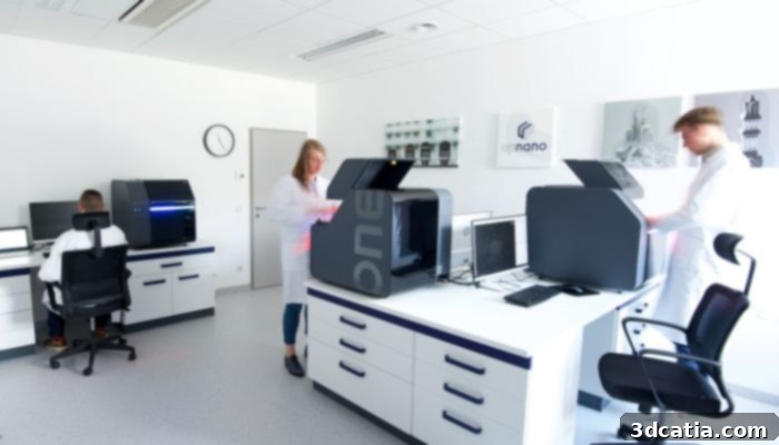
In close collaboration with customers, Markus Lunzer and his dedicated team at UpNano meticulously develop innovative 3D printing materials and refine application processes to meet diverse industrial and research needs, pushing the boundaries of additive manufacturing. (photo credits: UpNano)
Beyond the technical expertise, a substantial portion of our collaborations involves leading researchers from prestigious academic institutions worldwide. We are at the forefront of a highly innovative technology, 2PP, which is currently a vibrant and intensive area of scientific research. In this context, it is absolutely essential for our team to remain perpetually abreast of the very latest scientific developments, breakthroughs, and emerging trends within the 2PP field and broader additive manufacturing landscape. This requires continuous literature review, attending conferences, and engaging in scientific discourse. For me personally, the opportunity to continue engaging with scientific work is immensely rewarding and something I would not want to forgo; it keeps the intellectual curiosity alive and ensures we are always at the cutting edge. Our team is actively involved in numerous exciting and highly topical research projects, demonstrating the expansive reach of our technology. These projects span a wide range, from cutting-edge cancer research and intricate biomedical engineering applications, where precision, biocompatibility, and cellular interaction are paramount, to the development of novel high-precision manufacturing techniques for industrial innovation, such as creating micro-molds or specialized sensors. Through consistent scientific publications in peer-reviewed journals and presentations at international conferences, we are able to effectively communicate the remarkable capabilities and unique strengths of our technology to a global scientific and industrial audience. This not only showcases the transformative potential of 2PP but also contributes directly to the advancement of scientific knowledge and fosters new collaborations, cementing UpNano’s position as a leader in advanced additive manufacturing materials and applications. It’s a continuous cycle of discovery, application, and knowledge sharing.
3DN: What are the primary challenges you encounter as a Materials Engineer in this advanced field?
The overarching objective in our work is consistently to develop robust, reliable, and universally applicable solutions for complex problems. Our ultimate goal is to provide a solid, repeatable process that can be seamlessly integrated into industrial production workflows, moving beyond isolated laboratory prototypes to scalable, high-volume manufacturing. This pursuit of industrial-grade reliability often brings forth significant challenges, many of which tend to emerge only at advanced stages of product development. This is largely due to the exceptionally broad application scope of our technology; we are dealing with a vast range of dimensions, from intricate nanometer-scale features (e.g., for meta-optics) to larger centimeter-sized components (e.g., for microfluidic manifolds or medical devices), each presenting its own unique material and process demands, environmental factors, and post-processing requirements. A crucial aspect of our role, therefore, is the acute ability to recognize these nascent challenges – whether they relate to material stability, curing kinetics, mechanical properties, or surface adhesion – meticulously identify their underlying causes, and then leverage our collective expertise to devise effective, innovative resolutions. This systematic problem-solving approach is at the heart of what we do. I consider myself incredibly fortunate to be part of a team comprising exceptionally talented, passionate, and highly collaborative individuals. Many of our most successful solutions are not developed in isolation but through intensive, cross-functional collaboration with our software and hardware engineering teams. This interdisciplinary approach is absolutely critical because, in the realm of advanced 3D printing, the three core areas – material science (the ‘what’ is printed), software control (the ‘how’ it is printed), and hardware engineering (the ‘with what’ it is printed) – are profoundly and intricately interconnected. A minor change in one often necessitates significant adjustments or innovations in the others, demanding a holistic and integrated problem-solving strategy to achieve optimal performance, ensure reliability, and continuously expand the realm of application possibilities for our technology. The complexity is a constant challenge, but also a constant source of innovation.
3DN: What essential advice would you offer to someone aspiring to become a Materials Engineer in additive manufacturing?
For anyone considering a career as a Materials Engineer in the exciting and rapidly expanding field of additive manufacturing, my foremost advice would be to cultivate a continuous passion for learning and to stay profoundly informed about the latest trends, groundbreaking research, and technological advancements. The landscape of additive manufacturing is evolving at an exhilarating pace, with new materials, processes, and applications emerging constantly, and remaining updated is absolutely key to innovation and long-term success. However, it’s also important to acknowledge that there’s often a necessary, albeit subtle, shift in mindset when transitioning from academic training to an industrial role. In academic research, the primary drive is often to push the boundaries of what is conceptually possible, transforming what initially seems almost impossible into a tangible reality. This pursuit of fundamental discovery is undoubtedly impressive and serves as a vital catalyst for many subsequent technological developments, opening new avenues of exploration. In an industrial setting, while innovation remains utterly crucial, the emphasis subtly shifts towards creating solutions that are not only groundbreaking but also inherently reliable, stable, scalable, and economically viable for long-term production. It’s about building processes and materials that perform consistently, predictably, and robustly under diverse operating conditions, meeting strict industrial specifications and quality standards. Through practical experience, it frequently becomes clear that the simpler, more elegant solution is often not just more efficient in terms of development time, cost, and production scalability, but also proves to be more useful, robust, and universally adaptable across a wider range of applications. Therefore, developing a pragmatic approach, focusing on robust engineering principles alongside scientific discovery, is highly beneficial. Embrace active problem-solving, cultivate strong interdisciplinary communication skills, and always consider the full lifecycle, manufacturing feasibility, and scalability of your material innovations. The ability to bridge scientific theory with practical, industrial application is a highly valued trait in this field.

A materials engineer’s daily responsibilities involve recognizing intricate challenges, meticulously identifying their root causes, and proposing robust, innovative solutions during the development of new 3D printing materials for advanced applications, ensuring reliability and performance (photo credits: Rainer Fehringer)
What are your thoughts on the dynamic and crucial role of a materials engineer in the rapidly advancing field of additive manufacturing? We would love to hear your perspectives and experiences! Please share your insights and comments in the section below or engage with us on our vibrant social media platforms: LinkedIn, Facebook, and Twitter. Don’t forget to subscribe to our complimentary weekly newsletter here to receive the latest 3D printing news, groundbreaking innovations, and essential industry updates directly in your inbox! You can also explore our extensive collection of videos and in-depth tutorials on our official YouTube channel for more visual content and expert demonstrations. Your engagement helps us foster a thriving community around additive manufacturing!
*Cover Photo Credits: Markus Lunzer, UpNano