
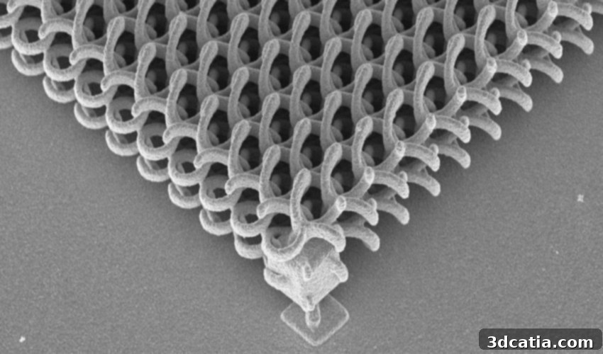
Revolutionary 3D Printing of Quartz Glass: Achieving Nanoscale Precision Without High-Temperature Sintering
The field of additive manufacturing has long sought to overcome the inherent challenges associated with 3D printing glass, particularly achieving high resolution and direct integration with sensitive components like semiconductor chips. A groundbreaking development from the Karlsruhe Institute of Technology (KIT) is now setting a new benchmark in this endeavor. A pioneering team led by Dr. Jens Bauer has successfully engineered an innovative 3D printing process for quartz glass, allowing for the creation of intricate nanometer-scale structures. What makes this advancement particularly remarkable is its ability to bypass the traditional, high-temperature sintering step entirely. Furthermore, these exquisitely detailed quartz glass structures can be printed directly onto semiconductor chips, a feat previously deemed impractical due to thermal constraints. This novel technique for 3D printing of glass heralds a new era, opening up a multitude of exciting and transformative possibilities across high-tech applications, advanced photonics, and precision micro-optics.
The genesis of this significant breakthrough lies within a powerful collaborative framework. The University of Heidelberg and KIT’s Institute of Nanotechnology (INT) have forged an alliance, establishing the prestigious Cluster of Excellence 3D Matter Made to Order. This initiative is dedicated to pushing the boundaries of additive 3D manufacturing processes, aiming to elevate them to unprecedented levels of capability and versatility. Within this ambitious framework, Dr. Jens Bauer, head of the IFT (Institute of Functional Interfaces) research group, along with his dedicated team, has made a decisive stride towards achieving the cluster’s overarching goals. This achievement was further bolstered by invaluable collaborations with scientists from the University of California Irvine and the medical technology company Edwards Lifesciences, also based in Irvine, underscoring the interdisciplinary nature and global impact of this research.
Historically, the additive manufacturing of quartz glass has predominantly relied on techniques centered around sintering. While effective for many applications, sintering silica-based nanoparticles demands extremely high temperatures, typically reaching around 1100 °C. Such intense heat presents a formidable obstacle, making it fundamentally incompatible with the delicate fabrication processes of semiconductor chips. The high thermal budget means that applying 3D-printed quartz glass structures directly in microsystems technology becomes unfeasible, thereby preventing significant technological integration and the realization of advanced functionalities. The inability to print directly onto chips has severely limited the potential of glass 3D printing for next-generation electronic and photonic devices. In stark contrast, the innovative process meticulously developed by Dr. Jens Bauer’s research group operates at temperatures that are nearly half as high, effectively circumventing these critical thermal limitations and paving the way for revolutionary applications.
Unveiling the Innovation: 3D Printing Quartz Glass Structures via Laser Lithography
The foundation of this low-temperature, high-resolution 3D printing method for quartz glass lies in a meticulously engineered material and a precise additive manufacturing technique. To achieve their goals, the researchers at KIT developed a novel, in-house hybrid organic-inorganic polymer resin. This specially formulated liquid resin serves as the crucial starting material for the printing process. At its core, this resin is comprised of polyhedral oligomeric silsesquioxane molecules (POSS). POSS molecules are unique, tiny, cage-shaped silica structures, distinguished by their silicon-oxygen core and the organic functional groups meticulously attached to them. These organic components allow for precise manipulation and polymerization during the printing phase, while the inorganic silica backbone forms the basis of the final glass structure.
The selection of POSS as the foundational material is a key innovation. Traditional glass 3D printing often uses silica powders that require high-temperature sintering, or specialized glasses with lower melting points that may not offer the same optical clarity and chemical resistance as fused silica. POSS, however, provides a molecular-level precursor that is rich in silicon and oxygen, allowing for the formation of a pure silica network upon the removal of organic components. This approach eliminates the need for particle fusion and subsequent high-temperature densification, which is the essence of sintering. The organic groups on the POSS cages facilitate solubility in solvents and enable photopolymerization, making the resin suitable for lithography-based 3D printing techniques. This ingenious design of the starting material is what fundamentally differentiates KIT’s process from conventional methods.
With this specialized POSS resin in hand, the researchers employed a highly precise additive manufacturing technique known as dip-in-laser lithography (DiLL) for the 3D printing phase. DiLL is an advanced variation of stereolithography (SLA), a vat photopolymerization method where a liquid resin is selectively cured by a light source. In the DiLL approach, the object is built from the top down. A substrate is immersed into the liquid POSS resin, and a focused laser beam then traces the desired pattern, polymerizing and solidifying the resin layer by layer. The precision of the laser allows for the creation of incredibly fine features, essential for achieving nanometer-scale resolution. As the structure is formed, the polymerized areas adhere to the substrate, and the uncured resin remains liquid, ready for the subsequent post-processing steps.
Once the initial 3D-printed organic-inorganic nanostructure is successfully formed through DiLL, it undergoes a crucial thermal post-processing step. The printed object is carefully heated to a moderate temperature of 650°C in air, typically within a tube furnace. This controlled heating process serves a critical dual purpose: it effectively expels the organic components that were originally part of the base POSS resin, and simultaneously facilitates the bonding of the remaining inorganic silica components. This conversion phase is pivotal, transforming the hybrid polymer structure into a robust, purely inorganic silica network. The significantly lower temperature of 650°C, compared to the 1100°C required for traditional sintering, is what makes this entire process compatible with direct printing onto heat-sensitive substrates like semiconductor chips, thereby unlocking a vast array of new applications in integrated photonics and microelectronics.
Following the thermal treatment, a final post-processing step is performed to ensure the purity and integrity of the printed objects. The heated structures are immersed in an isopropanol-alcohol bath for approximately 20 minutes. This solvent bath is designed to dissolve any residual uncured resin that might still be present within or around the intricately printed structures. This meticulous cleaning ensures that only the fully cured and transformed fused silica structure remains, resulting in a complete and continuous micro- or nanoscale object with superior optical and mechanical properties. The combination of the innovative POSS resin, the precision of DiLL, and the carefully controlled thermal and chemical post-processing steps culminates in the production of high-quality fused silica structures.
The intrinsic nature of the POSS resin, being a silicon-oxygen molecular network, is central to the success of this process. It means that the final printed structures are, in essence, fused silica derived from pure silica, achieved without any sintering whatsoever and at remarkably low temperatures. This is a game-changer for applications demanding the pristine properties of fused silica but limited by thermal constraints. Dr. Bauer succinctly captures the profound impact of this innovation: “The lower temperature enables the free-form printing of robust, optical-grade glass structures with the resolution needed for visible-light nanophotonics, directly on semiconductor chips.” This statement underscores the dual advantage of lower temperatures and high resolution, which collectively empower the creation of advanced integrated photonic devices and next-generation micro-optical systems.
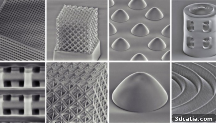
The innovative process developed at KIT was rigorously tested and validated on several complex 3D-printed quartz glass structures, showcasing its versatility and precision.
To thoroughly validate the robustness and versatility of their innovative method, the KIT team subjected the process to rigorous testing across a range of complex geometries. They successfully fabricated various nanoscale structures, demonstrating the precision and capability of their technique. Among the impressive examples were intricate photonic crystals composed of free-standing beams, precisely formed parabolic microlenses, and a sophisticated multi-lens micro objective featuring finely nanostructured elements. Each of these structures serves as a testament to the process’s ability to create functional optical components at an unprecedented scale and with exceptional detail. The results were consistently remarkable across all tests.
The nanometer-scale structures produced through this method consistently exhibited optically flawless and transparent glass, characterized by exceptionally high resolution. Beyond their optical superiority, these structures also demonstrated excellent mechanical properties, an essential factor for their longevity and reliability in demanding applications. The fused silica structures proved highly resilient, capable of withstanding challenging chemical and thermal conditions without degradation. Furthermore, a significant advancement was observed in resolution enhancement, achieving a fourfold improvement that is critical for enabling cutting-edge visible light nanophotonics. This level of precision allows for the manipulation of light at scales previously difficult to achieve with conventional glass manufacturing techniques. These outstanding results collectively unlock a myriad of potential applications across various high-tech sectors, positioning this novel process using the POSS material as a new global standard for micro- and nano-3D printing of inorganic solids. For those interested in delving deeper into the technical specifics and broader implications of this groundbreaking research, further detailed information can be found on KIT’s official website HERE.
The potential impact of KIT’s low-temperature, high-resolution 3D printing method for quartz glass is truly transformative. By enabling the direct integration of complex optical elements onto semiconductor chips, this technology paves the way for miniaturized, high-performance devices in fields such as telecommunications, medical diagnostics, environmental sensing, and even quantum computing. Imagine micro-scale spectrometers, integrated optical circuits for faster data transmission, or highly sensitive biomedical sensors, all manufactured with unparalleled precision directly onto the electronic brains of modern systems. This breakthrough promises not only to accelerate research and development in photonics and micro-optics but also to significantly reduce manufacturing complexities and costs by simplifying integration steps. The ability to customize glass components at the nanoscale with such ease could democratize access to advanced optical functionalities, fostering innovation across a broad spectrum of industries.
Do you think this new process developed at KIT will revolutionize glass 3D printing on the nanometer scale and accelerate the development of integrated photonics? We invite you to share your thoughts and predictions in a comment below or join the discussion on ourLinkedIn,Facebook, andTwitter pages! To stay updated with the very latest in additive manufacturing news, don’t forget to sign up for our free weeklyNewsletter here, delivering crucial 3D printing insights straight to your inbox! You can also explore all our informative videos and engaging content on our dedicatedYouTube channel.
*Cover Photo Credits: Dr.Jens Bauer, KIT