
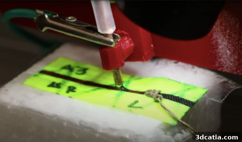
Revolutionizing Wearable Electronics: USF Pioneers 3D Printing Copper Directly on Fabric
The future of wearable technology is rapidly evolving, pushing the boundaries of what integrated electronics can achieve. In a significant leap forward, researchers from the Department of Electrical Engineering at the University of South Florida (USF) have secured both a patent and a substantial grant of $369,574 from the National Science Foundation (NSF). This pivotal funding is earmarked for the development of a groundbreaking method to 3D print copper directly onto fabric. This innovative electrochemical process, known as hydrogen evolution assisted (HEA) electroplating, marks a crucial milestone in the advancement of flexible, durable, and highly functional wearable electronics, paving the way for a new generation of smart textiles.
The rapid progression of electronic gadgets over recent decades has transformed them from bulky, single-purpose devices into sophisticated, multifunctional tools. Today, smartwatches track our health, headphones offer advanced audio and connectivity, and even computer glasses integrate digital information seamlessly into our vision. The next frontier in this evolution is the integration of electronics directly into our clothing. Imagine garments that can monitor vital signs, assist soldiers in combat, or provide critical data for astronauts in space. This is precisely the vision that Associate Professor Arash Takshi and USF Research & Innovation Interim Vice President and Professor Sylvia Thomas are pursuing with their pioneering HEA electroplating method. By enabling the direct printing of robust copper circuitry onto fabrics, their research opens up an abundance of technological innovations, promising a world where clothing is not just functional but also intelligently interactive.
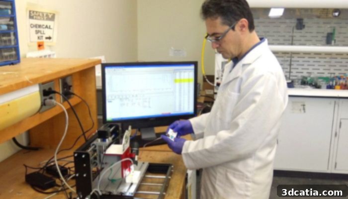
Professor Arash Takshi at Work (photo credits: USF)
The Innovative Hydrogen Evolution Assisted (HEA) Electroplating Process
The newly developed method for creating wearable electronics with copper 3D printing is an elegant two-step additive manufacturing process designed to overcome the limitations of existing technologies. The first step involves utilizing advanced laser printing technology to apply a highly precise conductive template to the fabric. During this stage, the fabric undergoes a controlled carbonization process. This carbonization is critical; it not only prepares the surface for subsequent steps but also significantly enhances the fabric’s stability and durability, making the integrated electronic components more resilient to wear and tear.
Following the template application, the second crucial step involves electroplating copper to produce a continuous, highly conductive copper pattern. This pattern meticulously forms the intricate circuit layout of the electronic component directly onto the fabric. A specially designed nozzle, integrated with a 3D printing device, facilitates localized electroplating. This precision allows for the targeted growth of copper, specifically in the junctions between the electronic components’ terminals and the printed circuit layout. A remarkable advantage of this method is the ability to solder these connections at room temperature, drastically reducing the risk of heat damage to delicate fabrics often associated with traditional soldering techniques.
What truly differentiates Takshi and Thomas’s HEA electroplating method from previous approaches lies in its unique electrochemical mechanism. The process involves increasing the voltage applied during electroplating. This elevated voltage simultaneously induces water electrolysis, leading to the evolution of hydrogen gas, alongside the growth of copper. This concurrent reaction has profound benefits: it significantly accelerates the copper deposition process and, perhaps even more importantly for wearable applications, enhances the mechanical stability and adhesion of the printed copper structure to the fabric. The result is a more robust, flexible, and long-lasting electronic circuit directly integrated into the textile, capable of withstanding the rigors of everyday use and movement.
Overcoming Limitations of Traditional Wearable Electronics
Professor Arash Takshi elaborates on the critical advantages of their HEA method, explaining, “The current technology for wearable electronics is mainly based on printing conductive inks consisting of nanoparticles of metals and/or carbon. The process relies on the physical connections of nanoparticles after drying the pattern. However, the high electric resistance from a conductive path made of conductive nanoparticles limits the applications to simple wearable electronic designs. These aren’t suitable for sensitive measurements and high electric current applications.” This statement highlights a major hurdle in the widespread adoption of advanced e-textiles. Conductive inks, while offering flexibility, often suffer from poor conductivity and can be prone to cracking or degrading over time, especially with repeated flexing and washing.
The HEA electroplating method directly addresses these issues by creating a continuous, monolithic copper pathway rather than a chain of connected nanoparticles. Copper, renowned for its exceptional electrical conductivity and mechanical robustness, provides a superior alternative. This two-step additive manufacturing approach allows for the creation of longer-lasting, more reliable wearable technologies without compromising the integrity of the underlying fabrics. Unlike traditional methods that might involve harsh chemicals or high temperatures that could damage delicate textiles, HEA electroplating offers a gentle yet effective way to embed complex circuitry, ensuring that the fabric remains flexible, breathable, and comfortable for the wearer while hosting sophisticated electronic functions. This breakthrough promises to unlock a new era of wearable devices capable of highly sensitive measurements and robust power delivery, expanding their utility far beyond basic activity tracking.
Vast Applications Across Diverse Sectors
With the recently granted patent and the significant financial backing from the NSF, this promising new method is poised for further development and rapid adoption across various sectors. The potential applications are incredibly diverse, spanning critical areas such as healthcare, military, and aerospace. In healthcare, this technology could revolutionize patient monitoring. Imagine smart garments capable of continuously tracking vital signs, body temperature, heart rate, and even more complex biochemical indicators, transmitting data wirelessly to medical professionals. Such proactive monitoring could enable early detection of health issues, provide crucial data for chronic disease management, and enhance telemedicine capabilities, ultimately leading to improved patient outcomes and more personalized care.
For military applications, the implications are equally transformative. Soldiers could be equipped with new generations of smart suits integrated with flexible sensors and communication systems. These suits could provide real-time situational awareness, monitor a soldier’s physiological state under extreme conditions, detect environmental hazards, and facilitate seamless communication. Such advanced wearable electronics could significantly enhance safety, efficiency, and operational capabilities in complex combat scenarios. Similarly, in the aerospace sector, astronauts could benefit from sophisticated suits that monitor their health and environmental exposure during demanding space missions, providing crucial data for their well-being and mission success. The ability to embed robust, flexible electronics directly into their attire could provide unprecedented levels of support and data collection in extraterrestrial environments.
Beyond these immediate high-impact sectors, the technology holds promise for a myriad of other fields. Athletes could wear smart sportswear that tracks performance metrics with unparalleled accuracy, providing real-time feedback for training optimization. The fashion industry could integrate interactive elements, dynamic lighting, or responsive features directly into clothing, blending technology and aesthetics seamlessly. The Internet of Things (IoT) stands to gain immensely, as nearly any textile surface could become a smart interface or sensor platform. While the researchers acknowledge that the technology still requires considerable hours of research and development before widespread commercialization, they are confident that this advancement is very likely to someday make our lives easier, safer, and more connected in countless ways, thanks to more easily achieved, robust, and versatile wearable electronics. You can delve deeper into the specifics of this exciting research by reading the official press release HERE.
What do you think of this groundbreaking new method for 3D printing copper on fabric? Share your thoughts and predictions in a comment below or join the conversation on our LinkedIn, Facebook, and Twitter pages! Don’t miss out on the latest advancements in additive manufacturing—sign up for our free weekly Newsletter here to get the freshest 3D printing news delivered straight to your inbox! You can also find all our insightful videos and demonstrations on our YouTube channel.
*Cover Photo Credits: USF