
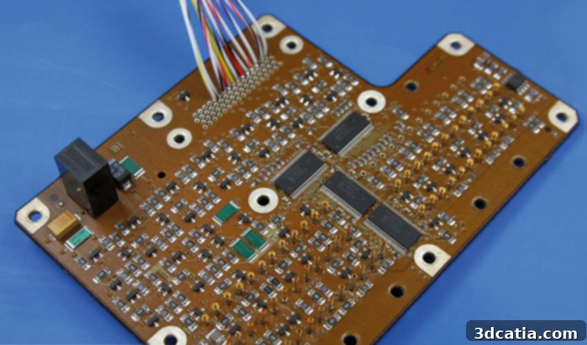
HENSOLDT and Nano Dimension Revolutionize Electronics with 10-Layer 3D Printed PCBs
The electronics industry, traditionally one of the slower adopters of advanced additive manufacturing technologies, is now witnessing a transformative shift. Sensor solutions provider HENSOLDT, in collaboration with Nano Dimension, a leader in Additively Manufactured Electronics (AME), has achieved a monumental breakthrough. This innovation marks a significant step forward in leveraging additive manufacturing for the development of high-performance electronic components. While the sector has gradually integrated AM for prototyping and small-batch production, this latest achievement by HENSOLDT and Nano Dimension demonstrates the unparalleled potential of 3D printing to enable new levels of customization and complexity for micro and nanoscale electronics components, pushing the boundaries of what was previously thought possible.
A Groundbreaking Achievement: The First 10-Layer 3D Printed PCB
At the heart of this groundbreaking development is the world’s first 10-layer 3D printed circuit board (PCB) that can successfully carry high-performance electronic structures soldered to both of its outer sides. This feat was accomplished by HENSOLDT using Nano Dimension’s newly developed dielectric polymer ink and conductive ink. The ability to solder components onto both sides of a 3D printed board represents a critical advancement. Until now, one of the significant limitations of 3D printed PCBs has been their inability to withstand the soldering process required for populating components on both sides, which is standard practice in conventional PCB manufacturing for achieving high component density.
This innovation is poised to open new avenues across numerous sectors demanding exceptional precision and performance. Thomas Müller, CEO of HENSOLDT, underscored the significance of this development, stating, “Military sensor solutions require performance and reliability levels far above those of commercial components. To have high-density components quickly available with reduced effort by means of 3D printing gives us a competitive edge in the development process of such high-end electronic systems.” This highlights the immense value of additive manufacturing in defense and aerospace, where custom, high-density, and robust electronic systems are paramount. The rapid availability of complex components directly translates into faster development cycles and improved operational capabilities, reinforcing national security and technological superiority.
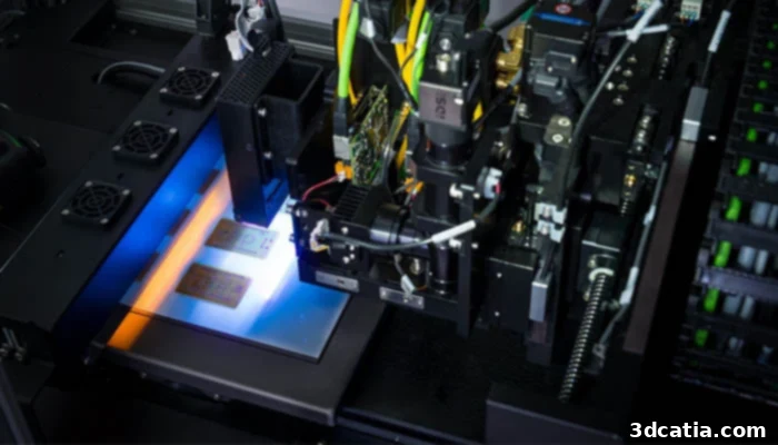
Nano Dimension’s technology can produce 3D printed circuit boards | Credits: Nano Dimension
Unpacking Nano Dimension’s Additive Manufacturing Technology
For several years, Nano Dimension has been at the forefront of developing and utilizing inkjet 3D printing technology specifically for the creation of electronic components. Their proprietary process is fundamentally based on photopolymerization. In this advanced method, their specialized printhead precisely deposits dielectric nanoparticles, conductive nanoparticles, and polymers onto a build plate. What makes this process truly innovative is the sequential curing: between each successive deposition of material, UV light is used to cure the deposited layers. This meticulous layer-by-layer construction enables the simultaneous creation of structures that are both highly conductive and perfectly insulating, which is crucial for the intricate design and functionality of modern electronic circuits. This unique capability allows for embedded components and complex geometries that are unachievable with traditional manufacturing methods.
The combination of these carefully selected materials – a newly engineered dielectric polymer ink and an advanced conductive ink – is what made the 10-layer PCB possible. The dielectric ink provides the necessary insulation between the multiple conductive layers, preventing short circuits and ensuring signal integrity, even at high frequencies. Meanwhile, the conductive ink forms the intricate traces and pads that carry electrical signals and connect components. The precision of Nano Dimension’s inkjet system ensures that these materials are deposited with extreme accuracy, creating fine features and multi-layer structures with exceptional fidelity. This technological prowess is what underpins the breakthrough, allowing for the creation of functional PCBs with a complexity previously unimaginable for additive manufacturing.
Transformative Benefits of Additively Manufactured Electronics (AME)
The adoption of 3D printing in electronics brings a multitude of advantages that directly address critical challenges in product development and manufacturing. One of the most significant benefits is a dramatically shorter time to market compared to traditional methods of creating electronic components. Conventional PCB manufacturing often involves extensive lead times for tooling, prototyping, and iterative design changes, which can delay product launches. With AME, design iterations can be printed and tested rapidly, allowing for quicker validation and adjustments. This agility significantly accelerates the development cycle, empowering companies to innovate faster and respond more effectively to market demands.
Furthermore, 3D printing offers substantial cost reductions for prototypes and small series production. In traditional manufacturing, the initial setup costs for molds, stencils, and specialized equipment can be prohibitive for low-volume runs. AME eliminates many of these upfront expenses, making it economically viable for companies to experiment with new designs and functions without committing to large-scale production investments. This affordability enables extensive testing of various designs before committing to final implementation, leading to optimized performance and reduced risk. Consequently, AMEs are invaluable for quickly verifying the functionality and design of specialized electronic components, resulting in a significant decrease in both time and cost throughout the entire development process. This extends beyond just PCBs to potentially include sensors, antennas, and other embedded electronic devices.
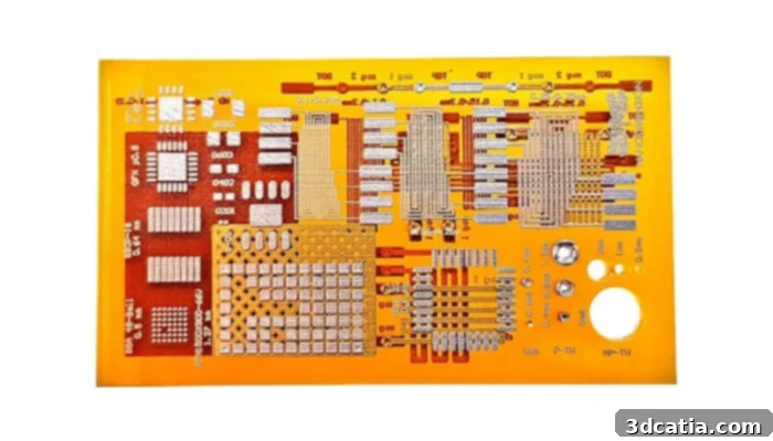
There is a great demand for printed circuit boards (PCBs) to become denser and more complex. The following PCB is multi-layer which means it contains multiple layers of conductive traces instead of containing only 1 | Credits: Nano Dimension
A Collaborative Journey: HENSOLDT and Nano Dimension’s Partnership
The success of this breakthrough is rooted in a long-standing and productive collaboration between HENSOLDT and Nano Dimension. HENSOLDT first began working with Nano Dimension’s DragonFly 3D printing system back in 2016, specifically to explore and understand the vast possibilities that 3D printing could offer for electronics manufacturing. This early engagement allowed HENSOLDT to gain deep insights into the technology’s capabilities and limitations, shaping the direction of future research and development. The ongoing partnership fostered an environment of continuous learning and innovation, crucial for tackling complex engineering challenges.
Building on this foundational work, HENSOLDT took another significant step last year by successfully implementing the DragonFly Lights-Out Digital Manufacturing (LDM) printing technology. The DragonFly LDM stands out as the industry’s only additive manufacturing platform designed for round-the-clock 3D printing of electronic circuitry, enabling unparalleled efficiency and productivity. This continuous operation capability is vital for accelerating development cycles and moving towards more industrialized applications of AME. Yoav Stern, President & CEO of Nano Dimension, eloquently summarized the synergy of this partnership: “Working together and learning from HENSOLDT led us to reach a first-of-its-kind in-depth knowledge of polymer materials applications. Additionally, it guided us in the development of Hi-PEDs (High Performance Electronic Device) that create competitive edges by enabling unique implementations with shortest time to market.” This statement underscores how the direct feedback and specific requirements from a high-performance electronics user like HENSOLDT were instrumental in refining Nano Dimension’s technology and materials, leading to the creation of truly High-Performance Electronic Devices (Hi-PEDs) that offer a distinct competitive advantage in the market.
The Future of 3D Printed Electronics and Its Impact
This milestone with the 10-layer 3D printed circuit board is not merely an engineering triumph; it’s a harbinger of a new era in electronics manufacturing. It signifies a future where electronic components can be designed and produced with unprecedented freedom, complexity, and speed. Beyond military sensor solutions, which initially drove much of this research, the implications are vast for industries such as medical devices, telecommunications, automotive, and consumer electronics. Imagine bespoke medical implants with integrated sensors, high-frequency antennas designed with ultimate precision for 5G/6G networks, or highly miniaturized components for next-generation smart devices. The ability to embed complex electronics within non-planar structures or create highly integrated systems in a single printing process will unlock innovation across countless applications, fostering more compact, lighter, and more efficient electronic systems.
The journey toward fully realizing the potential of Additively Manufactured Electronics is ongoing, but this breakthrough by HENSOLDT and Nano Dimension firmly establishes AME as a vital and viable technology for producing advanced electronic devices. It demonstrates that the challenges of material science and process control are being overcome, paving the way for wider adoption and new industry standards. As the technology continues to mature, we can anticipate even more sophisticated multi-layer structures, finer feature sizes, and a broader range of functional materials, leading to a truly digital and agile electronics manufacturing paradigm. This collaborative success underscores the importance of cross-industry partnerships in pushing the boundaries of what is possible, driving innovation, and accelerating the future of high-performance electronics.
What are your thoughts on this incredible 10-layer 3D printed circuit board and the future of Additively Manufactured Electronics? Don’t hesitate to leave your comments below or share your perspectives on our Facebook and Twitter pages! For all the latest news and advancements in 3D printing, sign up for our free weekly Newsletter and have it delivered straight to your inbox!
*Cover Image Credits: HENSOLDT